
TABLE OF CONTENTS
1. Introduction
2. Bill of Materials
3. Schematic
4. Code
5. ME Cad design
6. Final Thoughts
7. Download Original files
INTRODUCTION
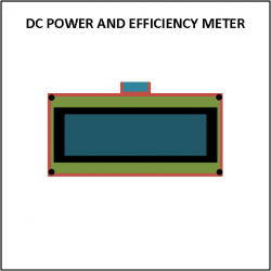
This is a fun little project that actually took me awhile to put together. What makes this project interesting and useful is that it will display your voltage, current, and power of any device you plug it into. What also makes this project useful is that it will calculate the efficiency of your device for example a dc dc converter.
The heart of this project is two INA219 high side current sensors from Texas Instruments. With this sensor you can measure up to 26V DC and up to +/-3.2A with a 0.1ohm shunt resistor (if you swap out the shunt with a 0.01ohm shunt you can measure up to +/-32A)
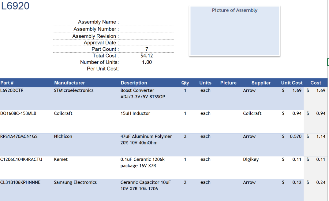
BILL OF MATERIALS
Click Here for bill of materials
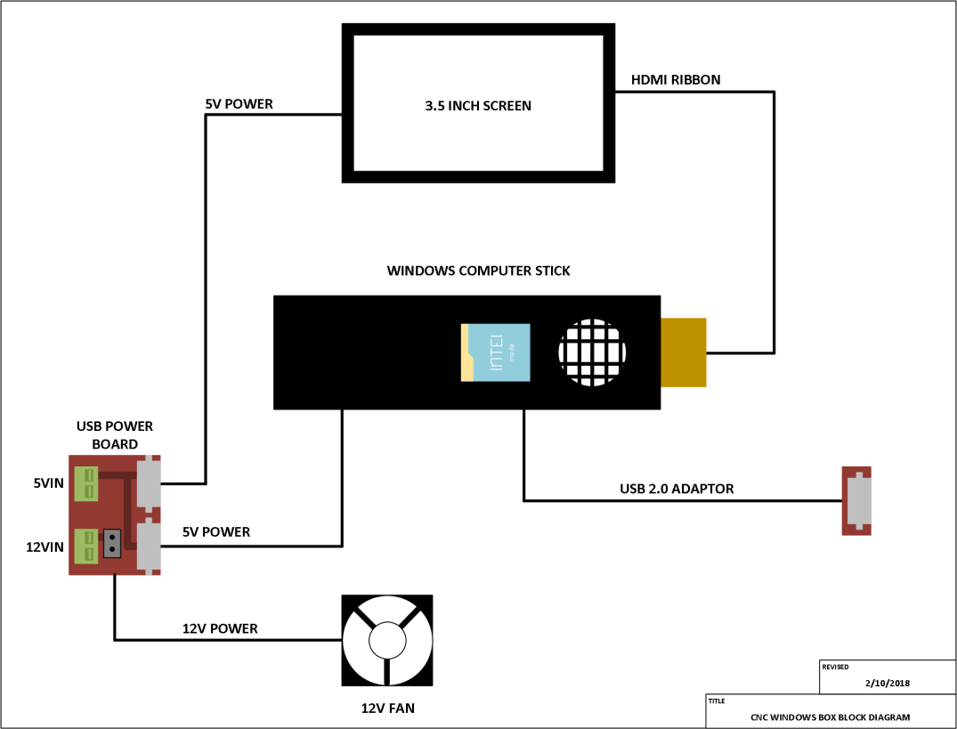
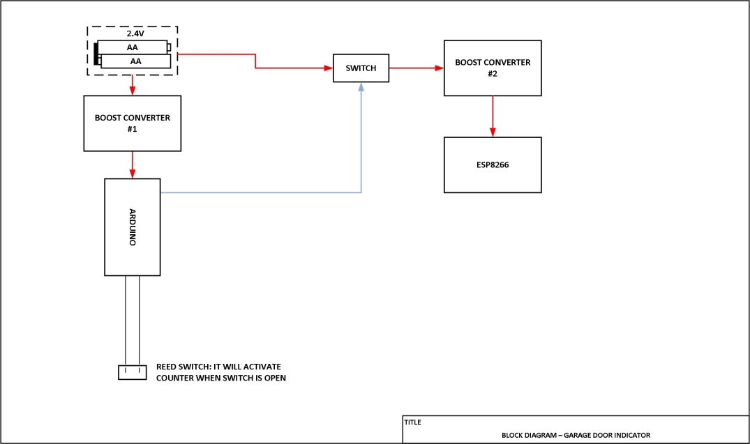
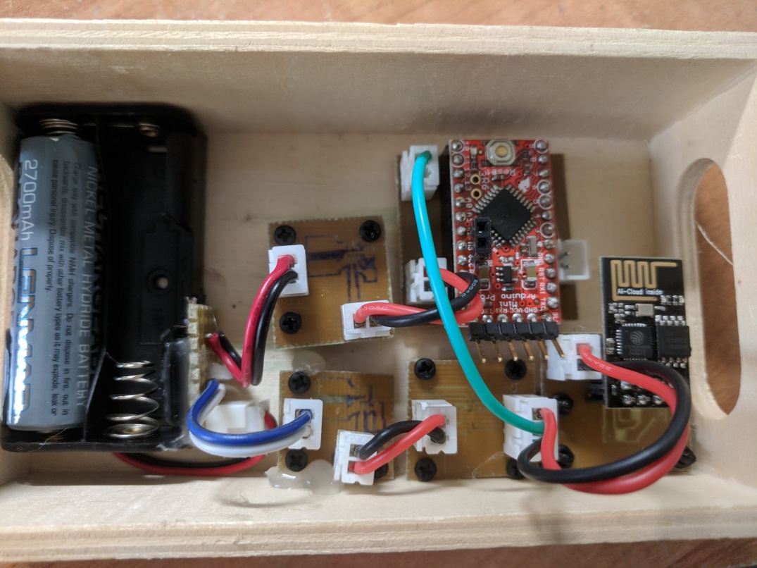
BLOCK DIAGRAM

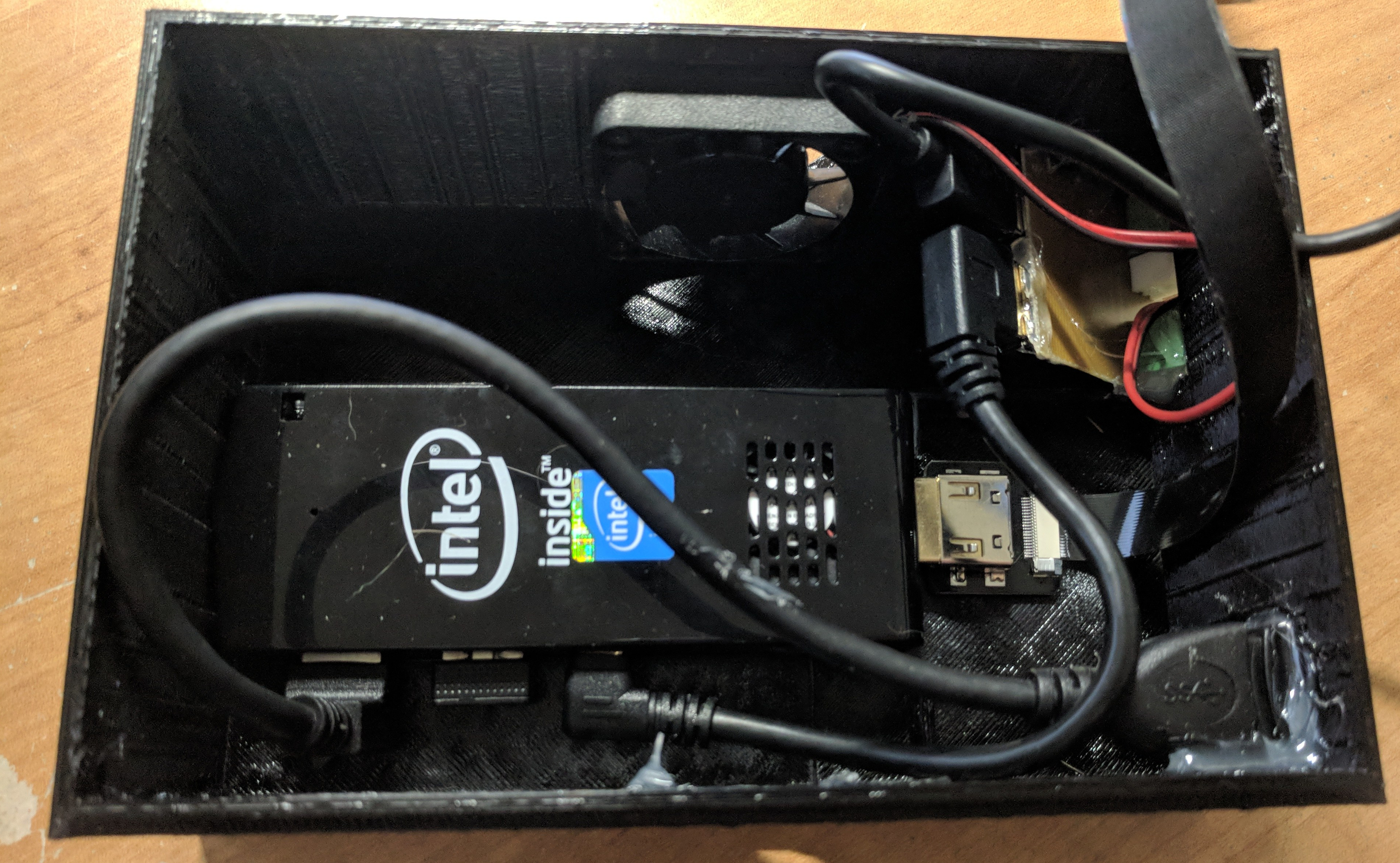
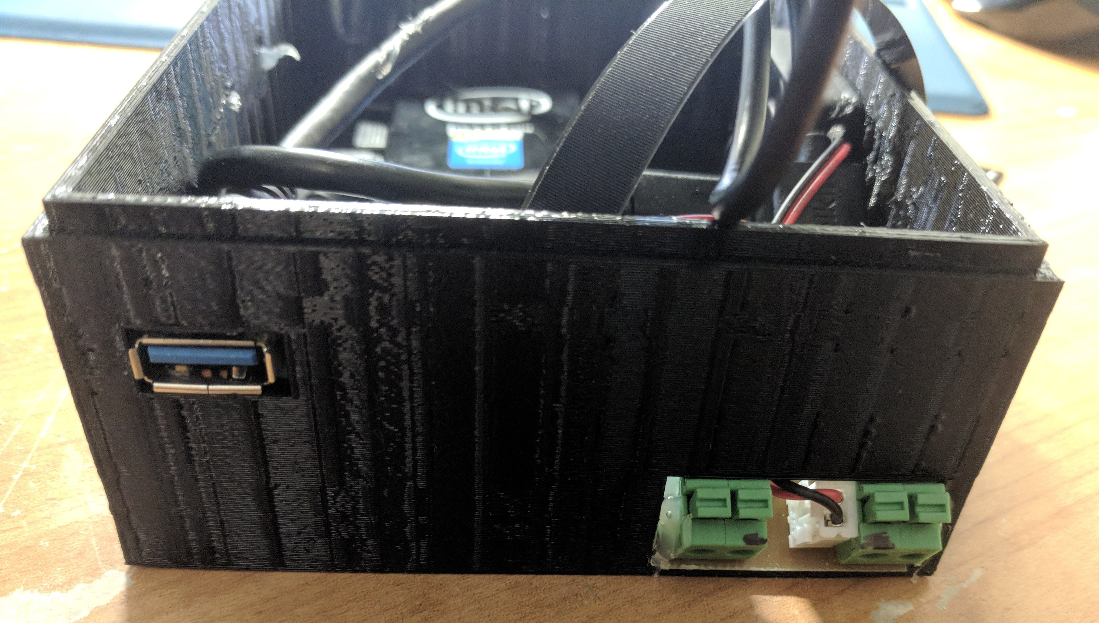
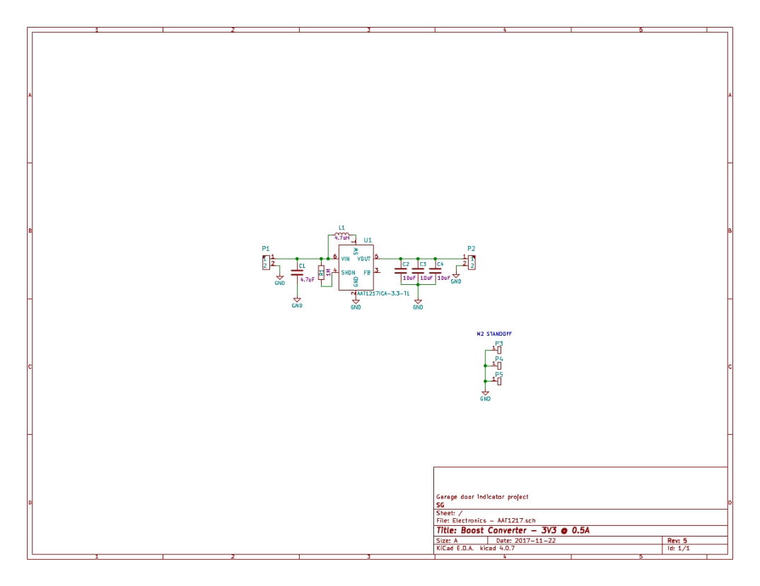
Here you can see a block diagram showing how I connected the different boards to create this project. Since I used my CNC machine to create the boards, it’s always much easier to separate the circuits into different boards for routing.
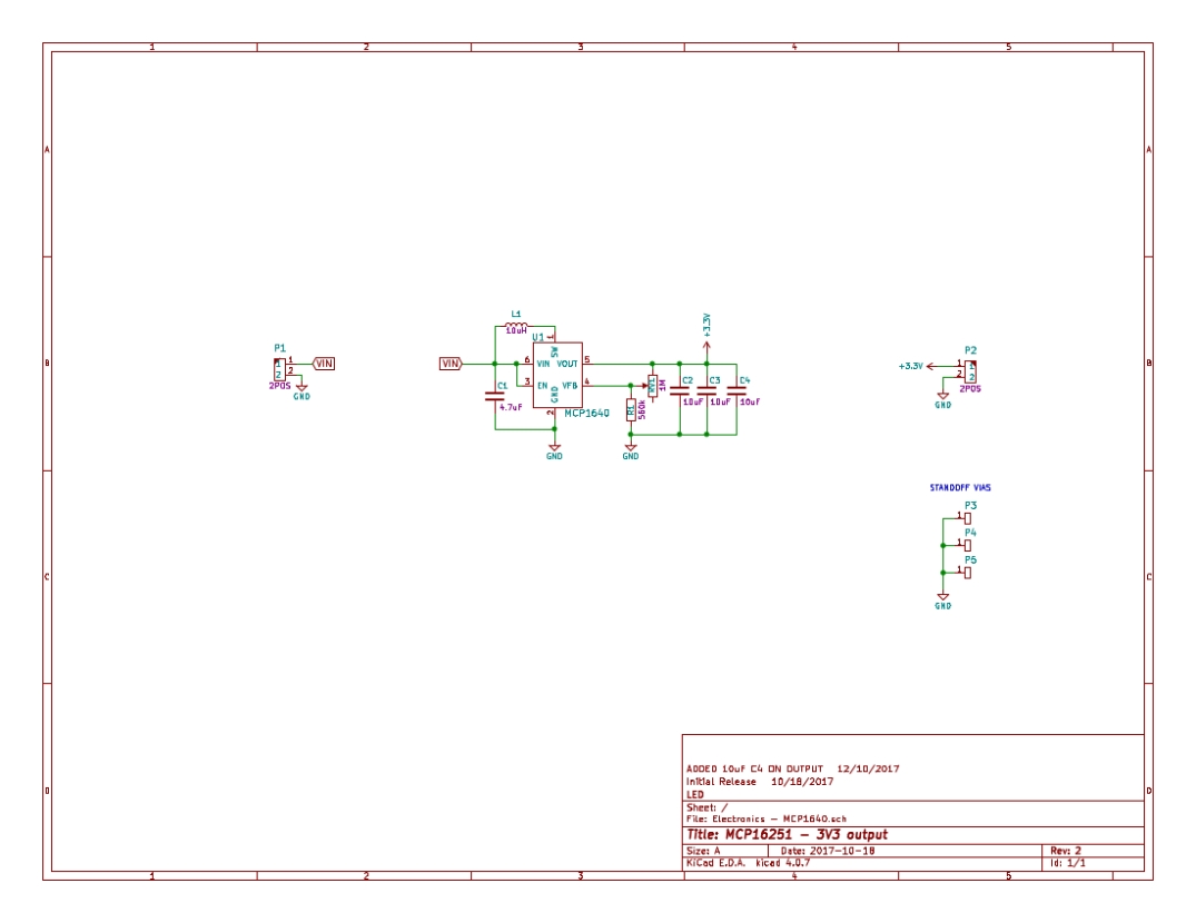
The main board consist of an arduino pro mini to keep the footprint as small as I can and also host a 5V boost converter being power from the 18650 lithium ion battery. In order to charge the battery without having to remove it from the enclosure, I decided to add a lithium ion charger board that connects in parallel with the battery. Its powered by a 5V USB mini connector and can be bought on amazon.
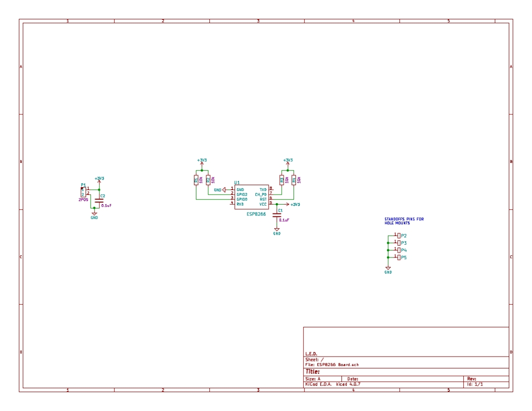
The second board host x2 INA219 high side I2C current, voltage, and power sensor by Texas Instrument. This IC is an amazing little thing because it takes a lot of the number crunching away from the Arduino and just sends the data over I2C that you need.
The final piece of this is the I2C liquidcrystal display for the arduino. I used this library here for the display. Make sure you connect the display and run an i2c address scanner on the examples for arduino because sometimes the displays have a different address than the default one listed.
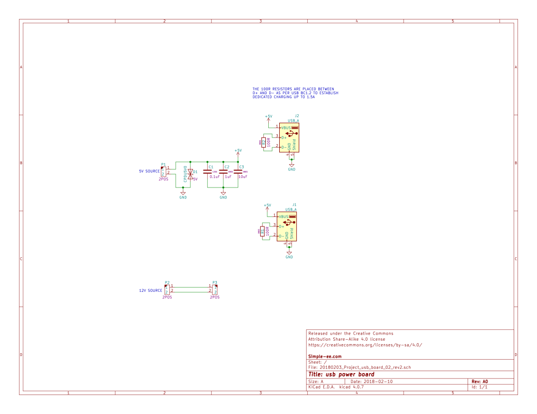
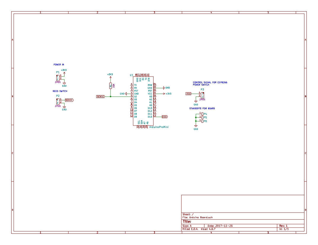
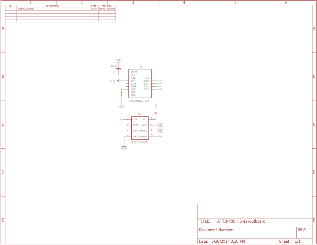
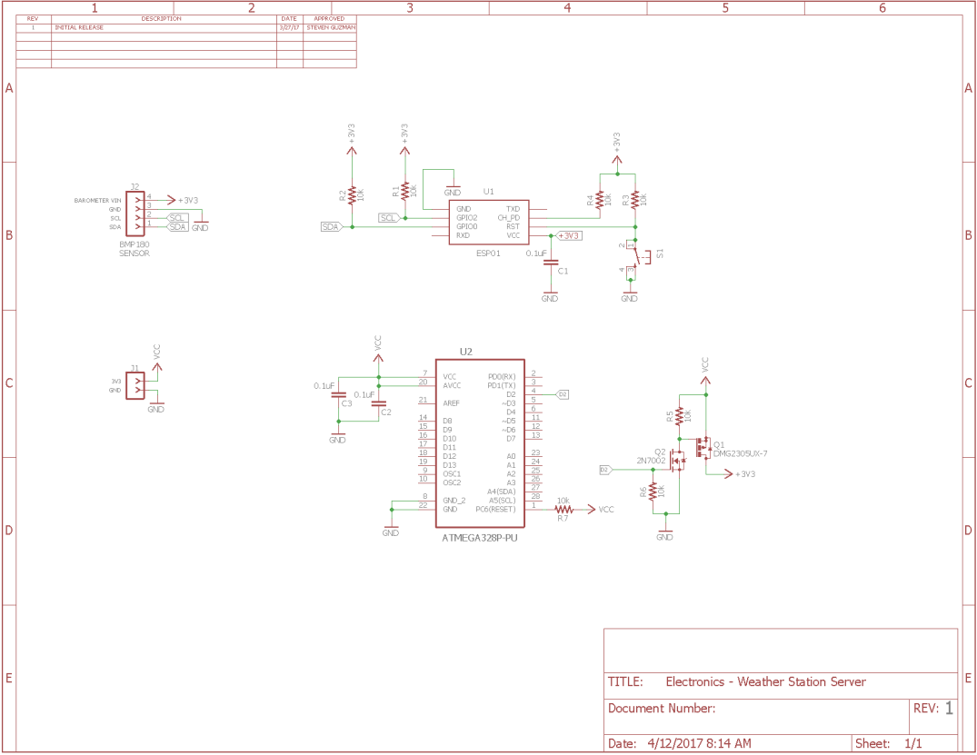
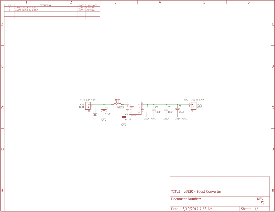
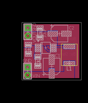
SCHEMATIC


CODE
/*

 * Name: Steven Guzman

 * Date: 2018/03/18

 * Description: This is a DC power meter that measures input and output

 *              power and calculates the efficiency of the system.

 *              It can also measure voltage and current of one or two

 *              voltage sources

*/

#include

#include

#include

LiquidCrystal_I2C lcd(0x3F,20,4); // Set the LCD address

/*

 * Below are the array values to store the measurements

 * and then used to convert float to string

 */

char float_volt1[8];  // voltage 1 array

char batt0[21];

char float_volt2[8];  // voltage 2 array

char batt1[21];

char float_current1[8]; // current 1 array

char curr1[21];

char float_current2[8]; // current 1 array

char curr2[21];

char float_eff[8];  // efficiency variable array

char line6[21];

char float_batt[6]; // battery voltage array

char line5[21];

// Analog sampling number

int sample = 20;

// Inialize current sensors.

// ina219_A default address is 0x40

Adafruit_INA219 ina219_A;

Adafruit_INA219 ina219_B(0x43);

// Variables to store current sensor data

float busvoltage1 = 0;

float busvoltage2 = 0;

float current_mA1 = 0;

float current_mA2 = 0;

float batt = 0.00;

void setup()

{

  Serial.begin(115200);

  while(!Serial)

  {

    delay(1);

  }

  ina219_A.begin();

  ina219_B.begin();

  lcd.init();

  lcd.init();

  lcd.backlight();

}

void loop()

{

  float xbat = 0.00;

  for(int x=0;x<sample;x++)

  {

    batt = analogRead(A0);

    xbat = xbat + batt;

  }

  // Read voltage levels from the voltage address

  // of the IN219 on both ICs

  busvoltage1 = ina219_B.getBusVoltage_V();

  busvoltage2 = ina219_A.getBusVoltage_V();

  // Read current levels from the current address

  // of the IN219 on both ICs

  current_mA1 = ina219_B.getCurrent_mA();

  current_mA2 = ina219_A.getCurrent_mA();

  // Average out the analog measurements

  // for the lithum ion battery voltage

  // sensing

  xbat = xbat/sample;

  float battery = xbat * (5.00/1024);

  dtostrf(battery,4,2,float_batt);

  sprintf(line5, "Battery:%-5s",float_batt);

  char temp3[] = "V";

  strcat(line5,temp3);

  // Convert float values into an char array to

  // better update on the lcd screen without

  // having to use the lcd.clear function

  dtostrf(busvoltage1,4,2,float_volt1);

  sprintf(batt0, "V1:%-5s",float_volt1);

  char temp2[] = "V";

  strcat(batt0, temp2);

  dtostrf(busvoltage2,4,2,float_volt2);

  sprintf(batt1, "V2:%-5s",float_volt2);

  char temp1[] = "V";

  strcat(batt1, temp1);

  // Convert mA to A readings

  float C1 = current_mA1/1000;

  float C2 = current_mA2/1000;

  dtostrf(C1,4,2,float_current1);

  sprintf(curr1, "C1:%-5s",float_current1);

  char temp4[] = "A";

  strcat(curr1, temp4);

  dtostrf(C2,4,2,float_current2);

  sprintf(curr2, "C2:%-5s",float_current2);

  char temp5[] = "A";

  strcat(curr2, temp5);

  float power1 = busvoltage1 * C1;

  float power2 = busvoltage2 * C2;

  float eff = (power2/power1)*100;

  dtostrf(eff,5,2,float_eff);

  sprintf(line6, "Efficiency:%-7s",float_eff);

  /*

   * Display on LCD screen all the values.

   * I used char arrays to update the values on the

   * screen.  Using the lcd.clear caused flickering

   * and was annoying.  With char array you can include

   * the units and it will update properly and not

   * overright the units.

   */

  lcd.setCursor(0,0);

  lcd.print(batt0);

  lcd.setCursor(11,0);

  lcd.print(batt1);

  lcd.setCursor(0,1);

  lcd.print(curr1);

  lcd.setCursor(11,1);

  lcd.print(curr2);

  lcd.setCursor(0,2);

  lcd.print(line6);

  lcd.setCursor(0,3);

  lcd.print(line5);

  delay(500);

}
There might be some issues with how wordpress displays the arduino code but I attached the original files at the end this tutorial.
As mentioned before, the libraries used here I obtained from other sources:
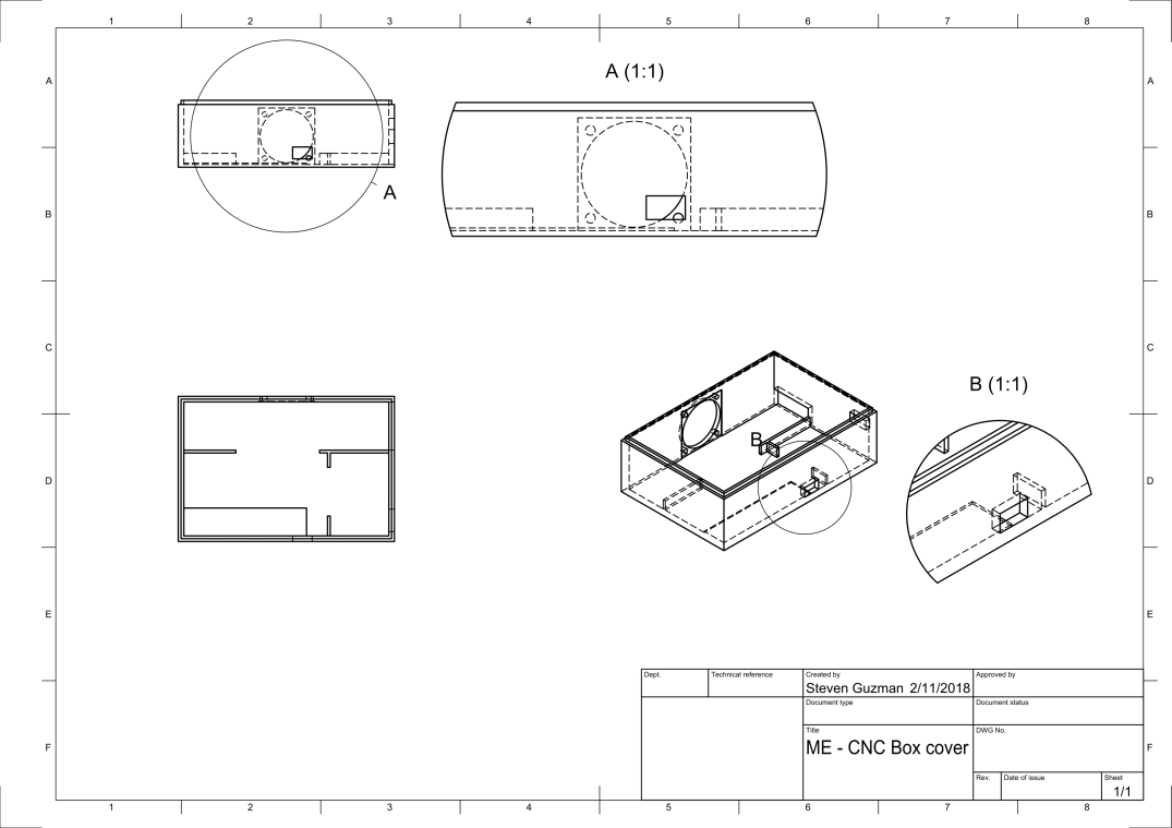
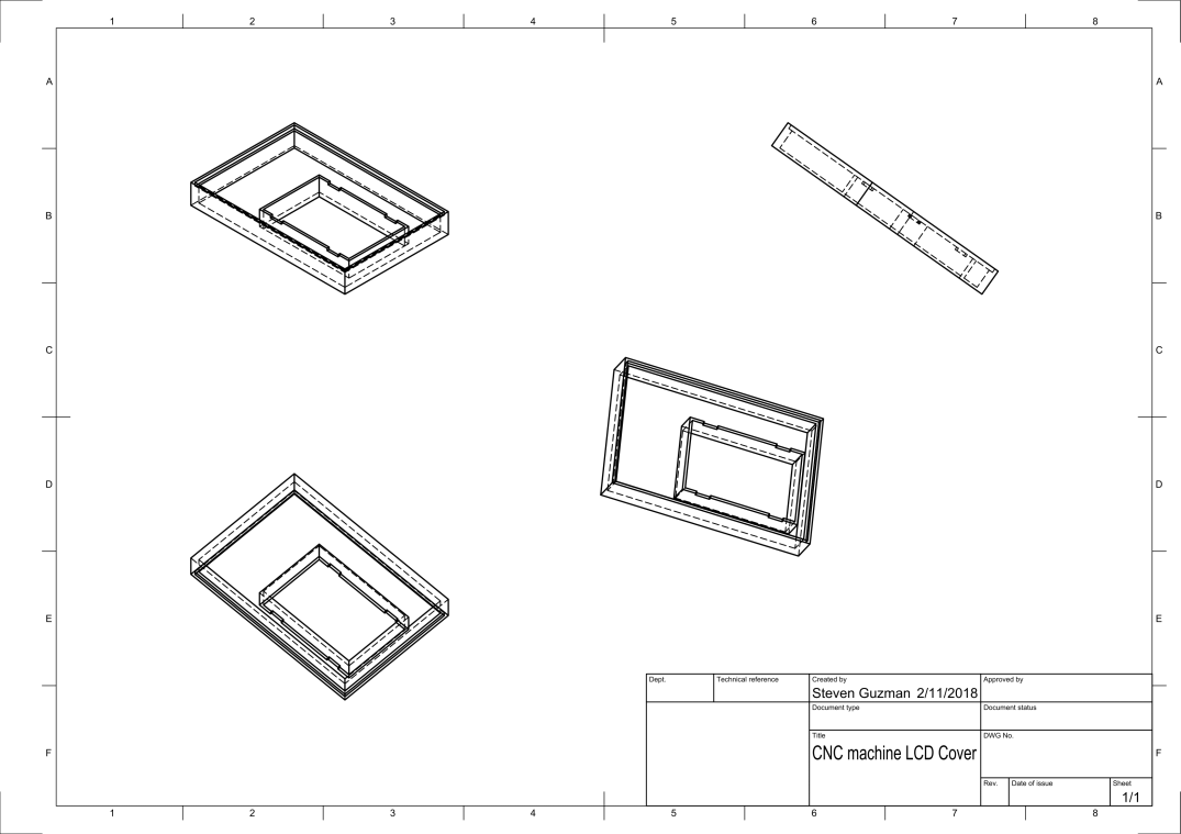
ME CAD DESIGN
I designed the enclosure in fusion 360 and printed the both with matterhackers pro series PETG red. I used a monoprice maker select v2 to print this enclosure.
Here is the step file for the enclosure
FINAL THOUGHTS


This was one of my favorite projects yet because the design alone makes me feel accomplished learning everything on my own. I still feel like I can make some upgrades to how I mount the internals and to be honest, I really rushed this part because I wanted to finish it.
Some upgrades I’m considering is using the arduinos internal 1.1V reference with a voltage divider to measure the battery voltage because it wasn’t as accurate as I wanted it to be.
Thank you for visiting and reading my project. if you have any questions or comments or suggestions please don’t hesitate to ask.


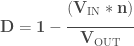
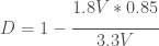
 . This is the most important part of the FET because in order to turn on the MOSFET you need to apply a voltage at the gate that exceeds this threshold voltage. In the datasheet of the MOSFET, you can find this value.
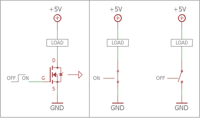


 = 0.52
 = 0.36
 = 0.22A
 = 0.165A
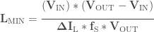
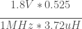
 – This is the switching frequency that the converter will operate at.
 = 3.72uH
 = 3.97uH
 = 0.19A
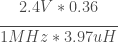 = 0.18A
 =
= 
 – This is the current switch limit of the boost converter.
 =
=  = 0.33A
 = 0.45A
 the Inductor will see. This value cannot exceed the ILIM value of the boost converter:
 = 0.94A
 = 0.72A
 value cannot exceed
  which can be found in the datasheet. In this example we see that with a low input voltage, the switching current exceeds the limit in the datasheet. The boost converter might still be able to output the desired current at that low input voltage because
 – This is the current that the feedback resistor draws.
 – This is the feedback reference voltage
 = 35mA
 = 35.4kΩ
 = 58.74kΩ
 : Typically this value is 4.7uF to 10uF
 – This is the maximum on time of the boost converter. It is also written as


 = 50uF
 = 50mV
 = 37mV
 = 87mV