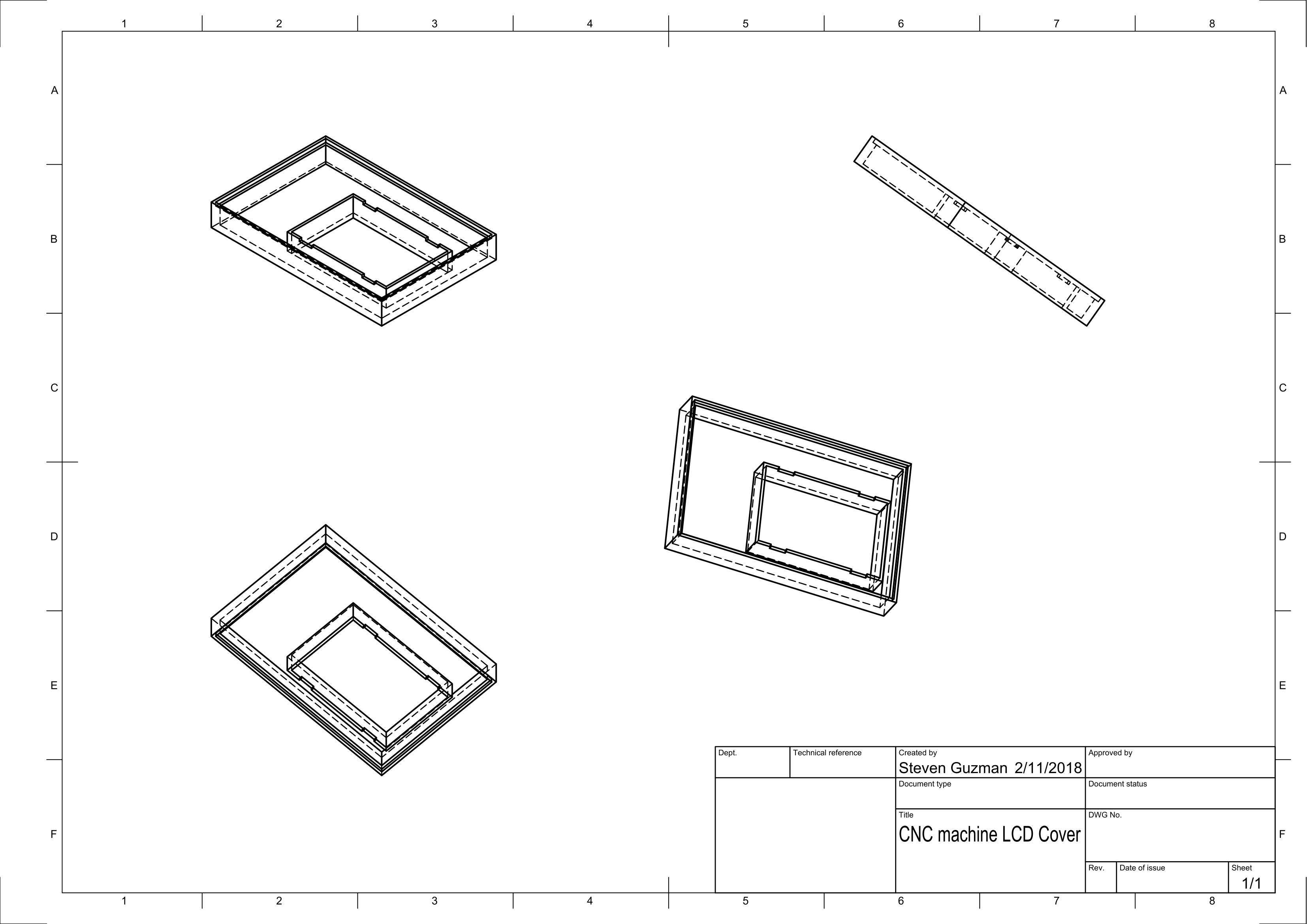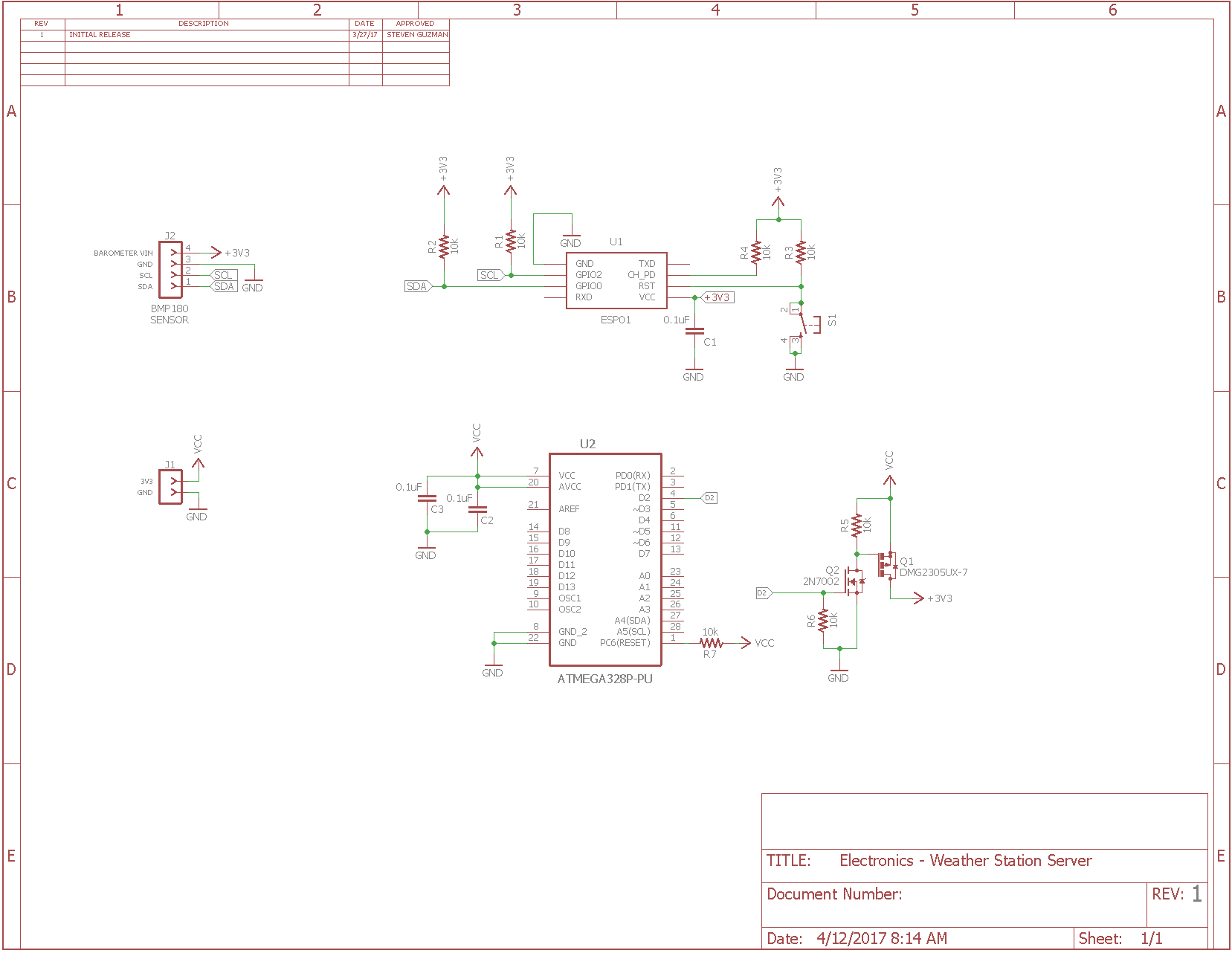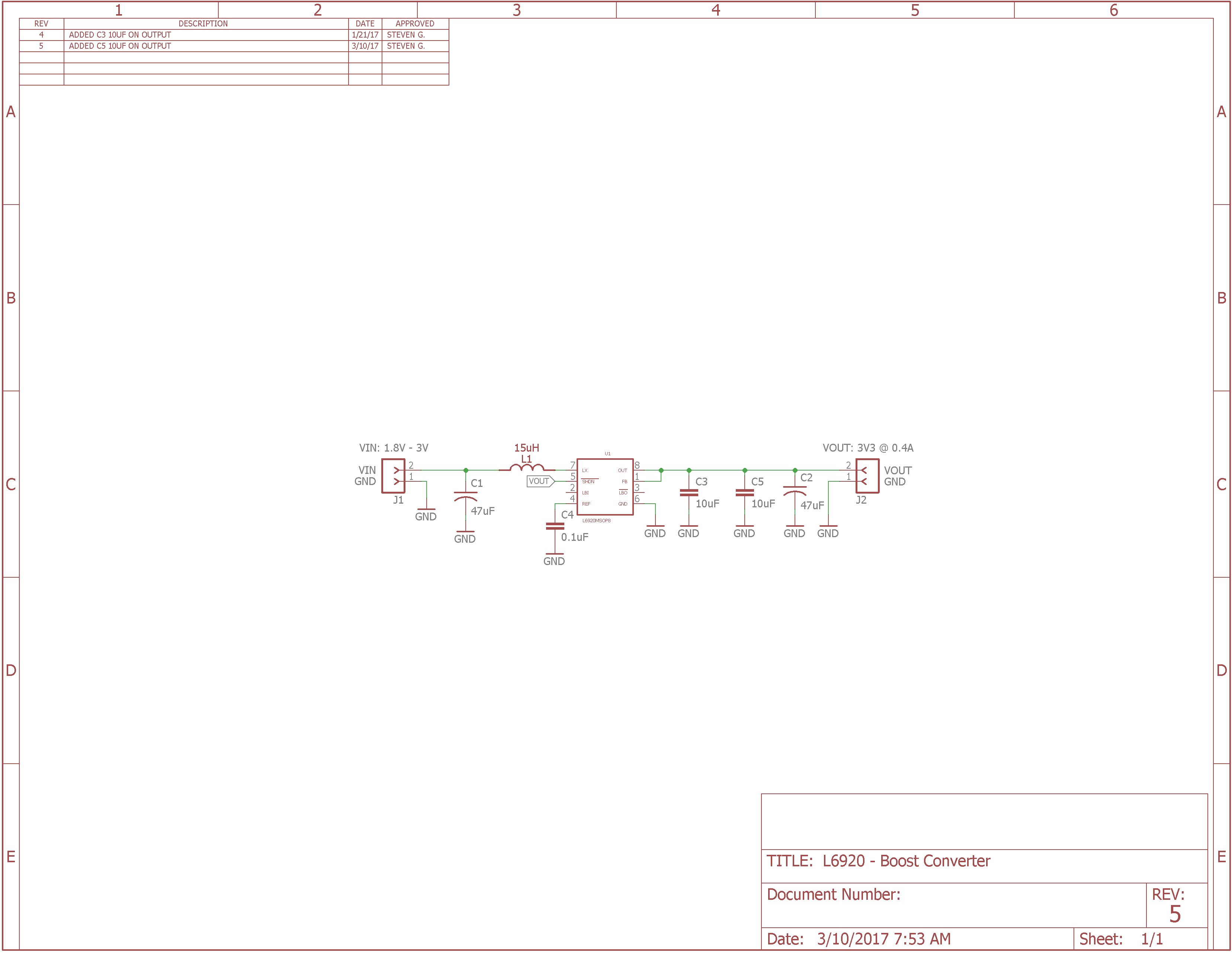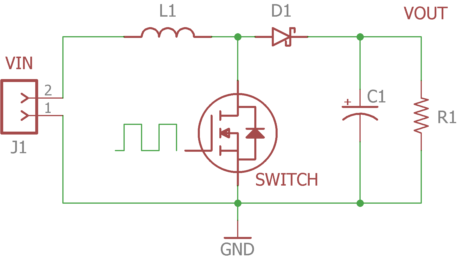
- Figure 1: Basic Boost Converter Circuit

Designing a boost converter sounds complicated and intimidating, well that was always my impression when it came to this topic in school. In reality, the design and testing of a boost converter is a lot easier than meets the eye.
Here I will walk you step by step on designing your first boost converter and how the datasheet is your best friend when designing. For this tutorial we will be using the L6920DC IC Boost converter from skyworks.[1]
Download the Boost Converter excel spredsheet from the Resources page.
This information was referenced from TI reference report.[2]
First and foremost, download the highlighted datasheet, datasheet-l6920dc. This has all the highlighted paremeters that you will need when designing a boost converter.
Step 1:
You need to decide what are your specifications. These are the key parameters:
- Vin(min)
- Vin(max)
- Vout
- Iout
- n = efficiency; Most boost converters average around 85 to 90% under medium load and up to 95% on heavy load. We will use the lowest percentage to be safe.
Example:
- Vin(min): 1.8V
- Vin(max): 2.4V
- Vout: 3.3V
- Iout: 0.4A
- n = 87% or 0.87
Step 2:
With your specifications, next step is to find your DUTY CYCLE:
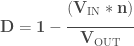
We calculated the duty cycle for both lowest input voltage and highest input voltage.
- Lowest input voltage gives you the highest switching current you will see
- Highest input voltage gives you the highest output current your converter can produce
Example:

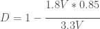 = 0.52

 = 0.36
Step 3:
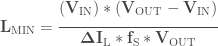
Next we will estimate the switching current or CURRENT RIPPLE of the Inductor:
ΔIL = 
Example:
ΔIL =  = 0.22A
ΔIL =  = 0.165A
Step 4:
Next we calculate the minimum INDUCTANCE we need:
 – This is the switching frequency that the converter will operate at.
Example:
 = 3.72uH
 = 3.97uH
We would select the highest inductance value to meet our input voltage rage of 1.8V-2.4V
When selecting the inductor, the key parameters you need to look for is low DCR, package size, and max current the inductor can handle.
DCR – Is the resistance in the coil because at the end of the day, an inductor is still a wire. When you keep this value at a minimum, it will increase your effieciency and the ability to provide a higher output power.
In step 7 , you will calculate the maximum current the inductor will see and there you will have all the necessary parameters needed to chose the inductor.
Step 5:
Now that we have our inductor value, we can calculate the actual CURRENT RIPPLE of the Inductor:
ΔIL = 
Example:
ΔIL = 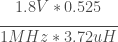 = 0.19A
ΔIL = 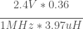 = 0.18A
Step 6:
Next we need to calculate the MAX OUTPUT CURRENT the boost converter can output:
 =
= 
 – This is the current switch limit of the boost converter.
Example:
 =
=  = 0.33A
=  = 0.45A
Step 7:
Next we will calculate the MAX SWITCHING CURRENT,  the Inductor will see. This value cannot exceed the ILIM value of the boost converter:

Example:
 = 0.94A
 = 0.72A
Note:  value cannot exceed
  which can be found in the datasheet. In this example we see that with a low input voltage, the switching current exceeds the limit in the datasheet. The boost converter might still be able to output the desired current at that low input voltage because is the minimum switching current it can handle. But better to be safe than sorry.
Here you can see the inductor will see a max of 0.94A at its lowest input voltage. Now we can chose the inductor for our design.
For this design I went with,MSS5131-472MLB, a 4.7uH inductor from coilcraft.[3]
Since I chose an inductor that has a higher value than previous calculated, the inductor current ripple and output power will be slightly lower but it will not effect your design negatively.
Step 8:
This step is only if your boost converter has an adjustable output voltage.
(This boost converter is a fixed output and does not require these resistors. Step 8 values are dummy values but the process )
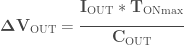
Here we will find R1 AND R2 values for the feedback network:

 – This is the current that the feedback resistor draws.

 – This is the feedback reference voltage

Example:
 = 35mA
 = 35.4kΩ
 = 58.74kΩ
Step 9:
Next l, we will calculate the INPUT CAPACITOR and OUTPUT CAPACITOR needed to minimize the ripple going in and out of the system:
First, you find your input capacitor:
 : Typically this value is 4.7uF to 10uF
Next, we need to first to look at these two equations below[6]:
 – This is the maximum on time of the boost converter. It is also written as

Were 

ESR – All capacitors are not ideal capacitors and therefore have what is known as Equivalent Series Resistance. This is an important parameter that you need to consider when choosing the right output capacitor.
Example:
Cin = 10uF
First, we need to choose a voltage ripple that we can live with. Here I chose 50mV, and if we rearrange the first equation, we get:
 = 50uF
Now we have a couple of options to choose from when it comes to materials for capacitors.
Most common are ceramic and electrolytic capacitors. Each have there own pro and con.
Ceramic capacitors offer lower ESR for lower ripple but they typically do not have the bulk capacitance.
Electrolytic capacitors have bulk capacitance but generally have a high ESR that adds to ripple.
In this case I decided to go with both, getting the benefit of bulk capacitance and low ESR.
I went with a 1206 package, 10uF ceramic capacitor and a 47uF Electrolytic in parallel. For the electrolytic, they also have an aluminum polymer that has high capacitance with the added benefit of low ESR. I went with a 47uF that has an ESR of 40mΩ.
Now we plug in the values we got back into the equations and we get:Special Note: For ceramic capacitors, you need to be careful of which class and package size you choose because you only see a certain percentage of your nominal value (ex. 1206 10uF X7R will see 73% of 10uF)[4]. Click here for more info. I generally go with 1206 or 1210 with capacitors.
 = 50mV
 = 37mV
 = 87mV
Always refer to the datasheet and compare recommended value vs calculated[1]
You’ve now designed your own boost converter regulator. See it wasnt too hard :).
I will post this project soon that has the schematic and bill of materials, it’ll be under the projects menu bar, stay tuned!!
Feel free to comment below and correct me if anything seems incorrect to you.
References:
1. L6920 Datasheet
2. TI Basic Calculations of a Boost Converter Power Stage
3. Coilcraft Inductor
4. Temperature and Voltage Variation of Ceramic Capacitors
5. Ceramic or electrolytic output capacitors
in DC/DC converters—Why not both?
6. Boost Converter Output Capacitor Selection