
Introduction
Like all my other projects, I’ve decided to create my own custom version of a cell monitor. Here we have an 8S arduino based voltage cell monitor that I designed to allow the user have control on how they monitor there batteries and how its displayed.
Its a very basic and not a lot of bells and whistles but still powerful enough to allow you to monitor cell voltages with accuracy and precision. This project is open source and so you will have the ability to add features or change them.
Specifications
- Cell count: 8
- Battery type: Li-ion, LiFePO4, NiMH
- ADC resolution: 16-bit
- Voltage measurement resolution: 1mV accuracy
- Fault detection: Over-voltage, Under-voltage
- I/O: 1-CH Digital output
The main purpose this is designed for is to measure an 8S Lithium Iron Phosphate pack up to 1mV resolution.
Hardware
Now here is were the fun part starts with the hardware used to create this DIY cell monitor. The main sections we will talk about are:
- ADC
- Power Supply
- MCU
- Menu Button Controls
ADC
Here we talk about the most important part of the project and that’s the ADC section. I’ve decided to go with two external 16-Bit adcs instead of the internal adcs of the arduino.
Since we need to step down the voltage from 30V max and need the best resolution possible. If we go with the internal adcs of the arduino, with a 10-Bit ADC we will only have resolution of 17mV/Bit. Now with 16-bit adcs, we have a resolution of 0.9mV/bit which is a huge increase.
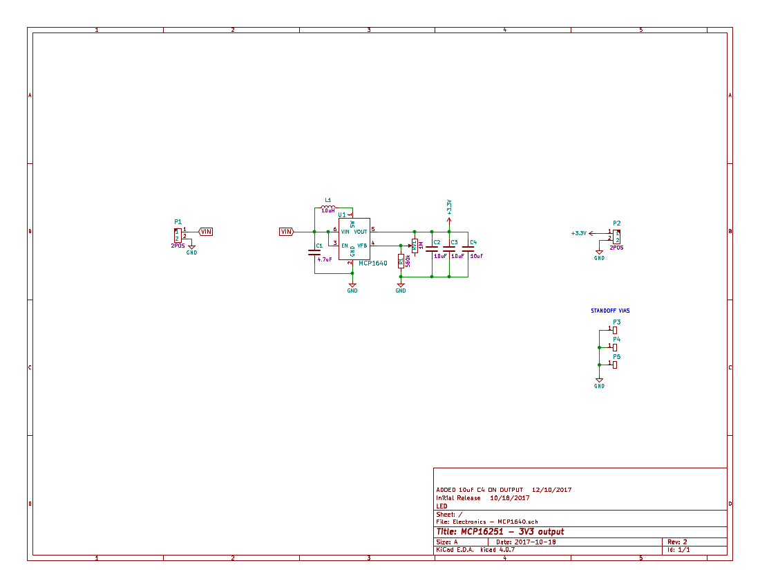
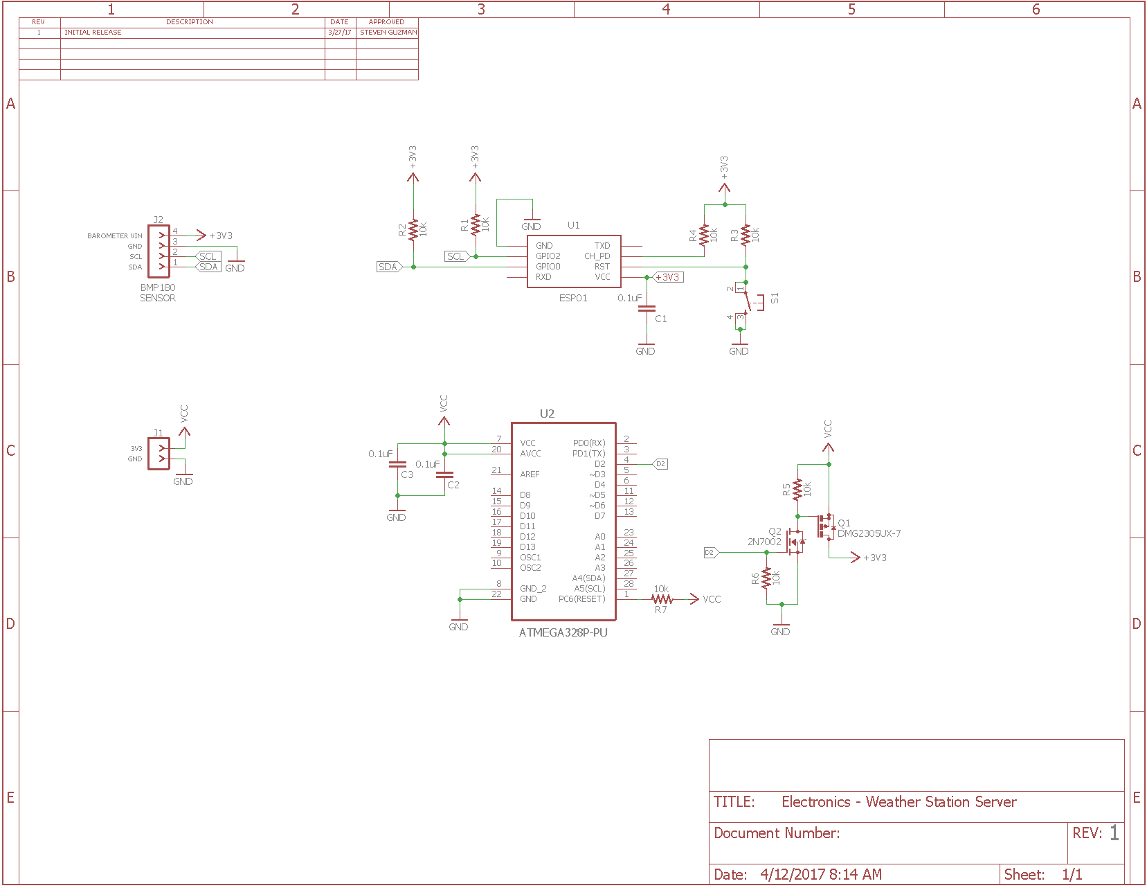
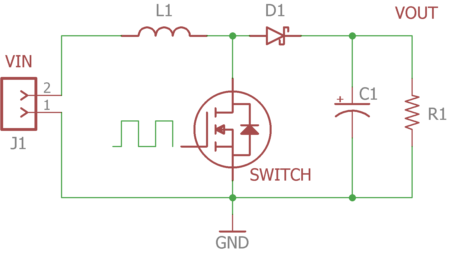
I’ve decided to go with the ADS1119IPWR which is a 16-bit I2C adc. See below for a snip-it of the schematic:

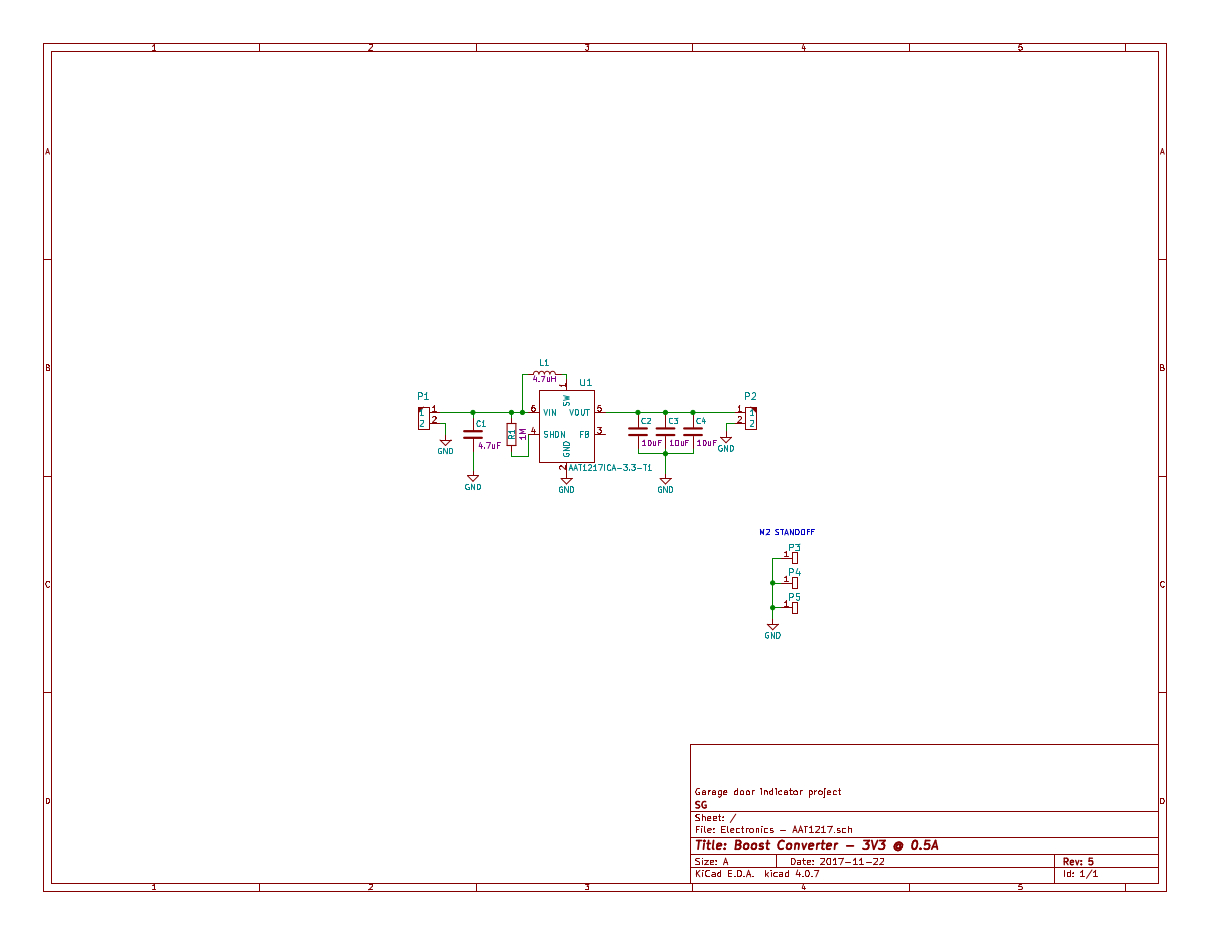
Power Supply
In the power supply section, we have a small profile buck converter that can handle up to 36V input. For this version I did not add a series fuse for the input of the buck converter but will add in second version. One this that was added was a tvs diode to protect the buck converter.
One thing I noticed is that when you plug anything into a high capacity battery bank, you need to protect your circuit from inrush current that causes a quick spike in current voltage that could damage your circuit before you even start. Adding a TVS diode will clamp this voltage and protect your circuit.

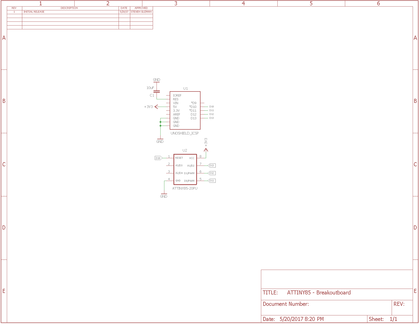
MCU
As the title implies, we are using the Atmega328P running the minicore bootloader https://github.com/MCUdude/MiniCore .
One thing I did change from the standard arduino board is use a cmos oscillator instead of the typical crystal oscillator. Honestly this is mostly a preference but it can be modified to use the typical crystal.

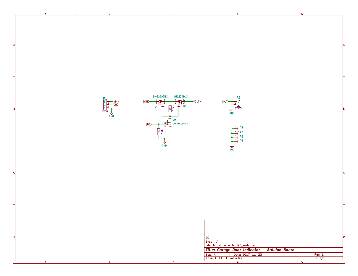
Menu Button Controls
Here is the schematic section for the control buttons. Its a little more complex than the typical push button design but this helps a lot with debounce.

We have a two stage design used to eliminate electrical debounce. First we have a passive RC low pass filter and then an inverting logic gate which adds some buffer to further reduce any false triggers.
Below is the full caption for all 4 input buttons:

Software
Normally I would breakdown every section of the code but its too large to fully go through the code. But I will go over the important sections:
- Menu controls
- ADC calibration
Menu Controls
In the control menu you are able to set the UVP value for cells and pack as well as the OVP value for cells and pack. In order to get into the menu screen you need to press the menu button and hold for about a second or two.
Once you are in the menu screen, you can navigate using the up and down buttons. Now even though I have the debounce circuit and a small software delay, the movement is still not smooth but it sufficient to operate.

In order to change the values, navigate for example to the OVP value with the arrow and then click the enter button to enter the OVP value screen. Using the up/down buttons you can increase or decrease the value by 0.05 increments. Once you are satisfied with your value then you can save the value by pressing the enter button and this will save to EEPROM so that its store permanently even after the power is removed.

ADC Calibration
Now before you can get accurate measured values, you need to calibration each ADC input to fix the offset from each IC.
You can calibrate using the serial monitor with an FTDI board connected to the UART port of the cell monitor.
The simplest way of calibrating each value is to measure each cell with a multimeter and write down the values.
Next, in the serial monitor, you need to enter the following:
1002, (cell 1 value), (cell 2 value) , (cell 3 value), (cell 4 value), (cell 5 value), (cell 6 value), (cell 7 value), (cell 8 value)
example: 1002,3.111,3.154,2.967,3.546,2.567,3.222,3.234,3.555

Make sure not to include spaces as this will not calibrate if you do.
After the calibrate is complete, calibrated values are stored in EEPROM so that after power is removed then the board is still calibrated.
Conclusion
Even though you can buy an 8S lithium battery monitor with probably more features, this one gives you more flexibility and also the confidence that its doing what it is suppose to do.
If you have any comments, suggests, or feedback let me know in the comments below. Thank you.
Here is the link to the schematics and code on my github:
https://github.com/simple-ee/CellMonitor


 = 0.52
 = 0.36
 = 0.22A
 = 0.165A
 – This is the switching frequency that the converter will operate at.
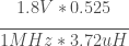
 = 3.72uH
 = 3.97uH
 = 0.19A
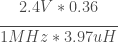 = 0.18A
 =
= 
 – This is the current switch limit of the boost converter.
 =
=  = 0.33A
 = 0.45A
 the Inductor will see. This value cannot exceed the ILIM value of the boost converter:
 = 0.94A
 = 0.72A
 value cannot exceed
  which can be found in the datasheet. In this example we see that with a low input voltage, the switching current exceeds the limit in the datasheet. The boost converter might still be able to output the desired current at that low input voltage because
 – This is the current that the feedback resistor draws.
 – This is the feedback reference voltage
 = 35mA
 = 35.4kΩ
 = 58.74kΩ
 : Typically this value is 4.7uF to 10uF
 – This is the maximum on time of the boost converter. It is also written as


 = 50uF
 = 50mV
 = 37mV
 = 87mV