Here is a new project I’m working on and hoping to get to a point where I can share the files and source code.
This is a replacement for a passive DC fuse box that you typically buy for low power solar projects.
This will allow you to remotely control 6 independent circuits each with a dedicated 25A max blade fuse. It uses an esp32 pico and each circuit has a 31A max current sensor. With the esp32, data logging can be incorporated and sent to influxDB server.
I’m very excited and hopefully I can get this project done so you can enjoy it as well
I strive to provide my content for free without using ads as I personally do not like ads in most website. If you can afford to donate anything via Paypal i would great appreciate it. Thanks:
INTRODUCTION:
This project was created in order to provide protection for my battery projects. I didn’t really trust the cheap low cost protection boards you find online so I decided to try and create my own.
The protection board I’ve designed has bidirectional current detection (can detect charging and discharging currents) which in turn means you can set independent OCP( over-current protection) for discharging current and charging current.
One thing to note before hand is that the current maximum current that can flow is about 5A due to lack of heatsink on the powerFETS. Adding heatsink is necessary to allow more current
Main features:
Over current protection with output latch open when tripped
Under voltage protection for the whole battery pack
Theoretically 45-50A pass-through current ( will require heatsink)
In the next sections I will discuss in more detail this project.
SPECIFICATIONS:
Here are some more technical details of this project
Minimum input voltage (V)
10
Maximum input voltage (V)
34
Maximum current (A)
50A*
Quiescent current (mA)
**
Undervoltage protection
Yes (adjustable)
Overcurrent protection
Yes (adjustable)
Short circuit protection
Yes***
Overvoltage protection
No
*Maximum current passing through this board will depend on sizing and adding a heatsink to the power mosfets
**Quiescent current has not been measured yet but it is below 1mA during normal operation with a 4S battery. This will change slightly when using more cells in series
***Theoretical the supervisor IC will latch when the overcurrent protection section detects its threshold. This will need testing to confirm
SCHEMATIC AND CIRCUIT DETAILS
Here in this section I will discuss the project in more detail by talking about the different sections used to create this whole circuit.
Lets first discuss the over-current/short-circuit protection sections of the circuit:
Bidirectional Current sensor
Here we have the heart of the over-current detection. We have the MAX4081FASA which is a bidirectional current sense IC that can handle a max VCC of 76V which is more than enough for our applications. The FASA has an internal gain of 5V/V coupled with a 10 milliohm sense resistor value ( I have two 20 milliohm in parallel for size reduction) this will allow the sense current of up to 50A.
REF1A is tied to 5V reference IC and REF1B to ground. With this we have a bias point of 2.5V meaning that when no current is passing the voltage on the OUTPUT pin 5 is 2.5V. When current is discharging into a load the output will rise up to 5V being the 50A max. When current is flowing the other direction to charge the batteries then it will go below 2.5V to 0V being 50A max.
In order to both detect charging and discharging current since I will be using this for a battery pack, I had to create a circuit that detects both an upper limit and lower limit. Hence I went with a window comparator to detect charge and discharge values.
Window comparator with latching supervisor IC
Here is where you can adjust your own over-current detection points for charging and discharging and they can be set independently from each other. The idea here is when the output from the max IC is within the window of the voltage values you set from the voltage divider values on pin 3 and pin 6, the output of the opamp will be high. As soon as the output value goes above or below those set points, it will pull the output of the op-amp low and trigger the supervisor IC.
The supervisor IC is very important because this is what controls the power mosfets allowing current to pass through. This one is different from normal supervisor ICs because when this triggers, the output is latched low and this pulls the power mosfets high causing them to stop current flow. The only way to clear the fault condition is to pull the clear pin 1 to 5V. What I have done is add the option for a push button on the board directly or pads to run the clear pin trigger somewhere else.
Here is a simple equation to calculate the discharge current detection resistor values on PIN3 of the op amp:
(0.05 V/A * X) + 2.5V = VdetectHigher ; X = current trigger desired
For charging current detection here is the equation for the lower voltage detection of the op amp PIN 6
(0.05 V/A * X) – 2.5V = Vdetectlower; X = current trigger desired
Here is the power mosfets controlled by the supervisor IC. When no fault condition is triggered then the supervisor IC pulls Q4 to high causing the 10k resistor to be tied to ground. This then creates a voltage difference between the gate and source for the powerFETS allowing current to flow. When an overcurrent fault condition is triggered the supervisor IC is then pulled low and Q4 stops conducting which in turns unties the 10k resistor from ground and makes the gate and source the same potential.
Now the under-voltage protection scheme works by using a different supervisor IC measuring the input voltage. When the voltage falls below the threshold then the output pulls low and stops current flow in the powerFET
Here you see this circuit in action. A voltage divider is used to bring down the input voltage of the pack to a range the supervisor can handle. I have defined some voltage divider resistor values for different size battery packs in which it will trigger when the threshold is hit. I only used one MOSFET for this because this will stop discharging current but will allow charging current to flow via the body diode until the input voltage is above the threshold and then turn on the mosfet.
Here you have to take some precautions not to kill the mosfet when an event triggers an under-voltage event and you try to charge the pack.
When an event happens, start charging the pack with 0.5A-1A until there is about 1V above the under-voltage value. Then maximum current charging can be applied. This part of the circuit will need more tweaking in the future
CONCLUSION / IMPROVEMENTS
Hopefully this project will help someone out. I created this to help protect my batteries and to allow the flexibility to adjust as much values as I can and have as much control of my protection circuitry as possible. Of course this is not perfect and I am still working on improvements.
IMPROVEMENTS:
Figure out a way to protect Under-voltage powerFET from getting damaged when charging through the body diode initially until the supervisor IC allows current to flow through the FET and not the body diode
Use DPAK powerFETS instead of IPAK due to cost. Size increase is negligible or non-existent
Create a heatsink to provide maximum current discharge through mosfets. Currently the maximum current discharge without heatsink is roughly 5A without getting too hot. Will do testing after its completed.
With the Arduino mini, there is a need for a USB to UART controller to upload your sketches and this could also be used for the ESP8266.
This project is inspired and based off the Sparkfun’s FT231X breakout board design. I’ve created this project because 1. I like designing and soldering electronics 2. Try to create a cheaper alternative to the popular FT232RL and also add 1 or 2 features to the current FT231X breakout board.
BILL OF MATERIALS
For the bill of materials, its pretty straight forward. I’ve attached links to digikey for each component as I find them easier to order from but you could also get the parts from arrow or mouser as well.
Below I’ve attached an image of the schematic but i’ve also attached the original kicad files and a PDF version of the schematic at the end of the post.
OSHPARK
If you feel like you want to get this board made, I’ve attached a link to my oshpark project. With oshpark, I find they make great quality boards at a great price for small sized boards.
FINAL THOUGHTS
I know this was a short post and project but I found it important to share another option for those’s who want to find a cheaper solution and want to learn along the way. You can find a lot cheaper solutions on amazon that are china made but i’ve read stories in some cases that they were not genuine FT232RL ICs. If you wish to build your own, its very easy and rewarding at the same time.
In the next revision I will add LEDS for TX and RX indication as for this version I eliminated to save some cost and space.
Arduino and the implementation of GRBL has allow for amazing things to be created. One of those things are low cost CNC machines that enable us to create anything we want.
I bought myself a low cost CNC engraver from amazon and after modifying it, it has been one of my best investments because as en electrical engineer I can create PCB boards to test my designs here at home and verify before getting them sent out. One problem I usually have is that I use my laptop to run the gcode software and my laptop is really big and sometimes a hassle to keep on my desk.
My solution was to create this project and make a standalone CNC machine controller to run the gcode software in a compact package. I tried fiddling around with using a raspberry pi 2 as my main PC but I’m still a beginner with raspberry pi’s and I had issues getting the settings right. My next option was to use a windows based machine and luckily I found just the solution.
In this tutorial I will explain how I put this together and what improvements could be made.
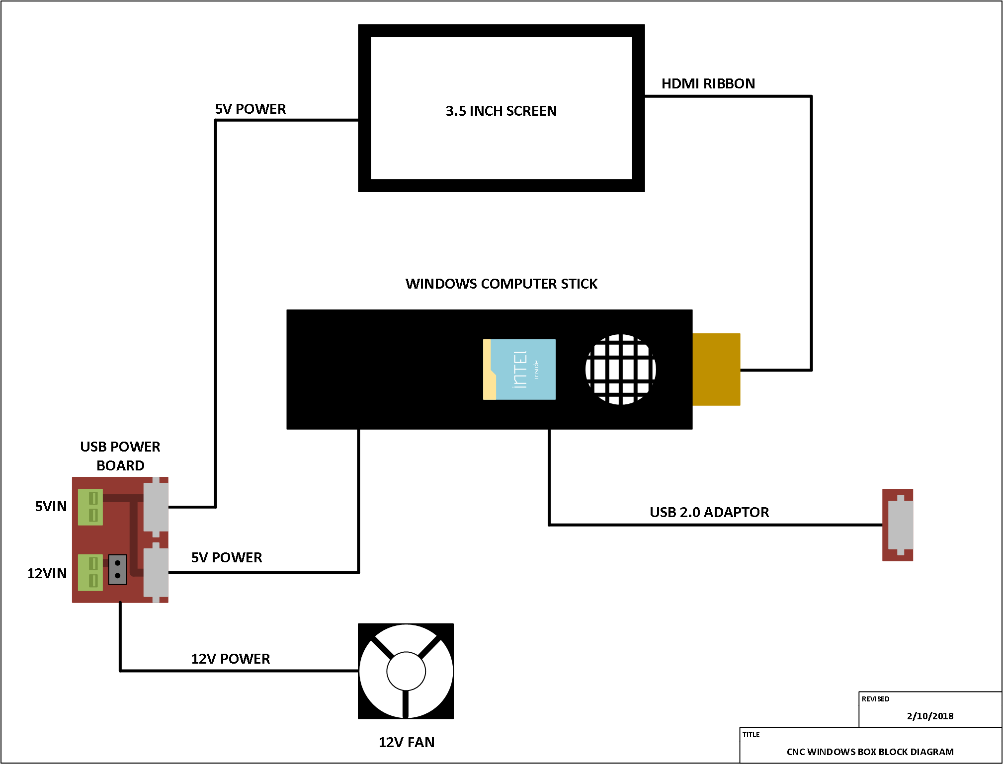
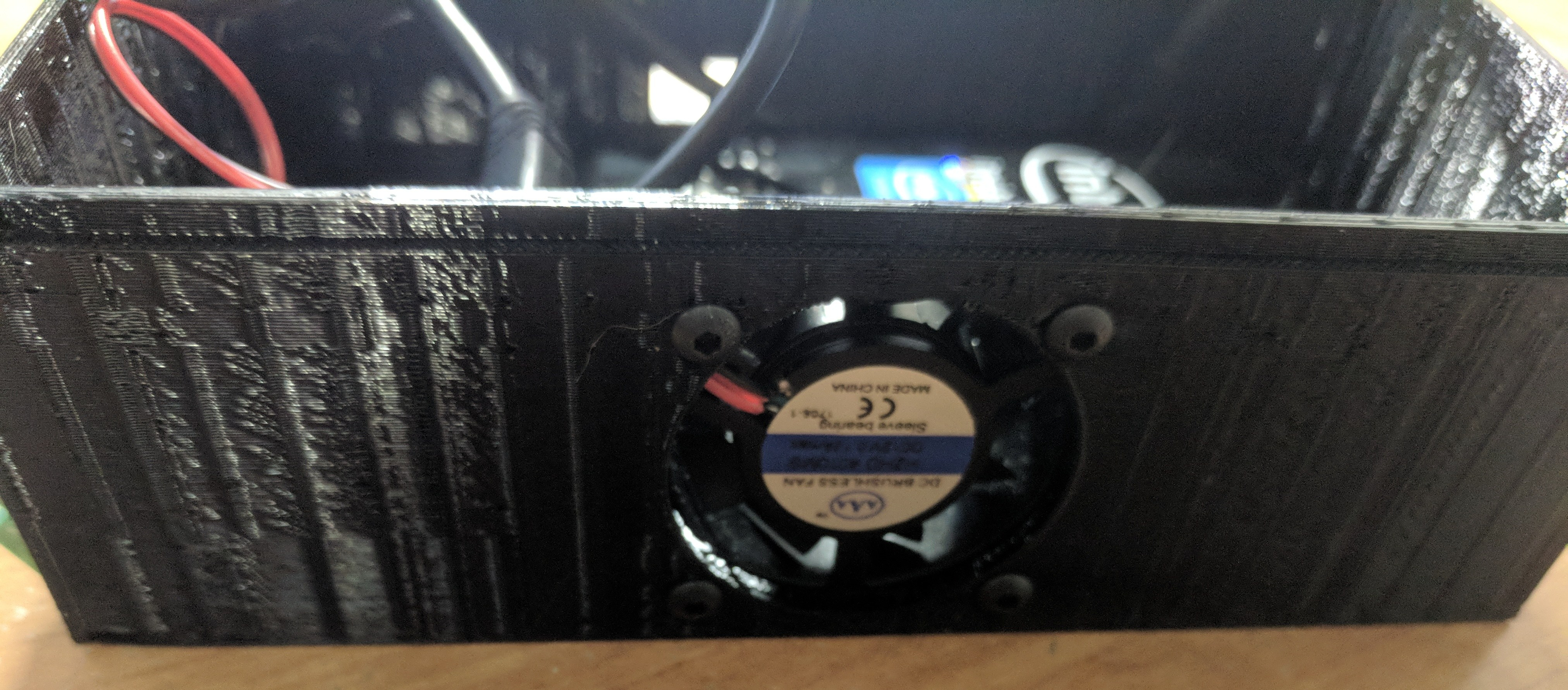
Here is the block diagram for how this project is wired. With the exception of the enclosure itself and the usb power board, everything was bought ready to go. I’ve added a fan as a just in case because the computer stick does generate some heat so the fan will prevent the system from over heating but so far it does not seem to be an issue with heat and therefore is an option.
The 5V and 12V supply are coming from my 24V power supply that powers my Arduino GRBL shield. What I did was use two step down converters 1) For 5V step down and 2) For 12V step down. I realized this might not be idle but it is my first revision of this project.
SCHEMATICS/ CAD DESIGN
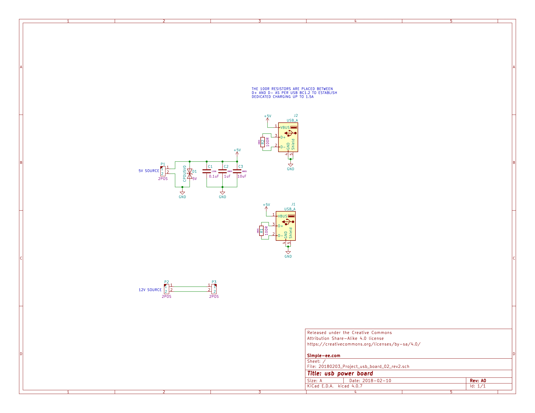
The only schematics I have is for the USB power board and I created that using Kicad. The board was basic, since both the screen and the windows computer stick ran on 5V via micro USB, I needed to distribute power from one source into two loads. To add some safety, I did add a TVS 5VWM diode to prevent over voltage spikes from destroying the devices along with some filtering capacitors.
If its a little blurry don’t worry because all original files will be included in a download link at the end.
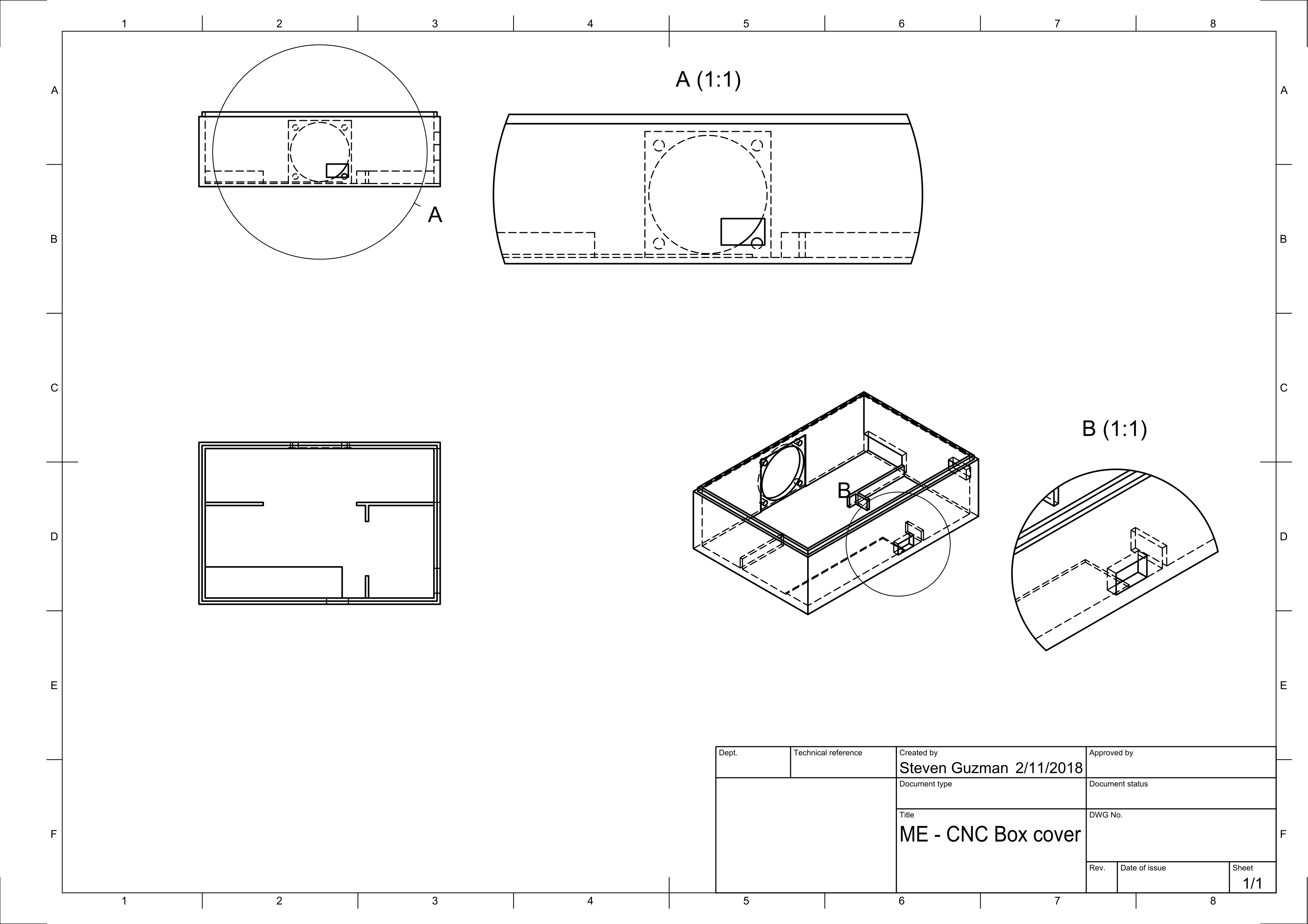
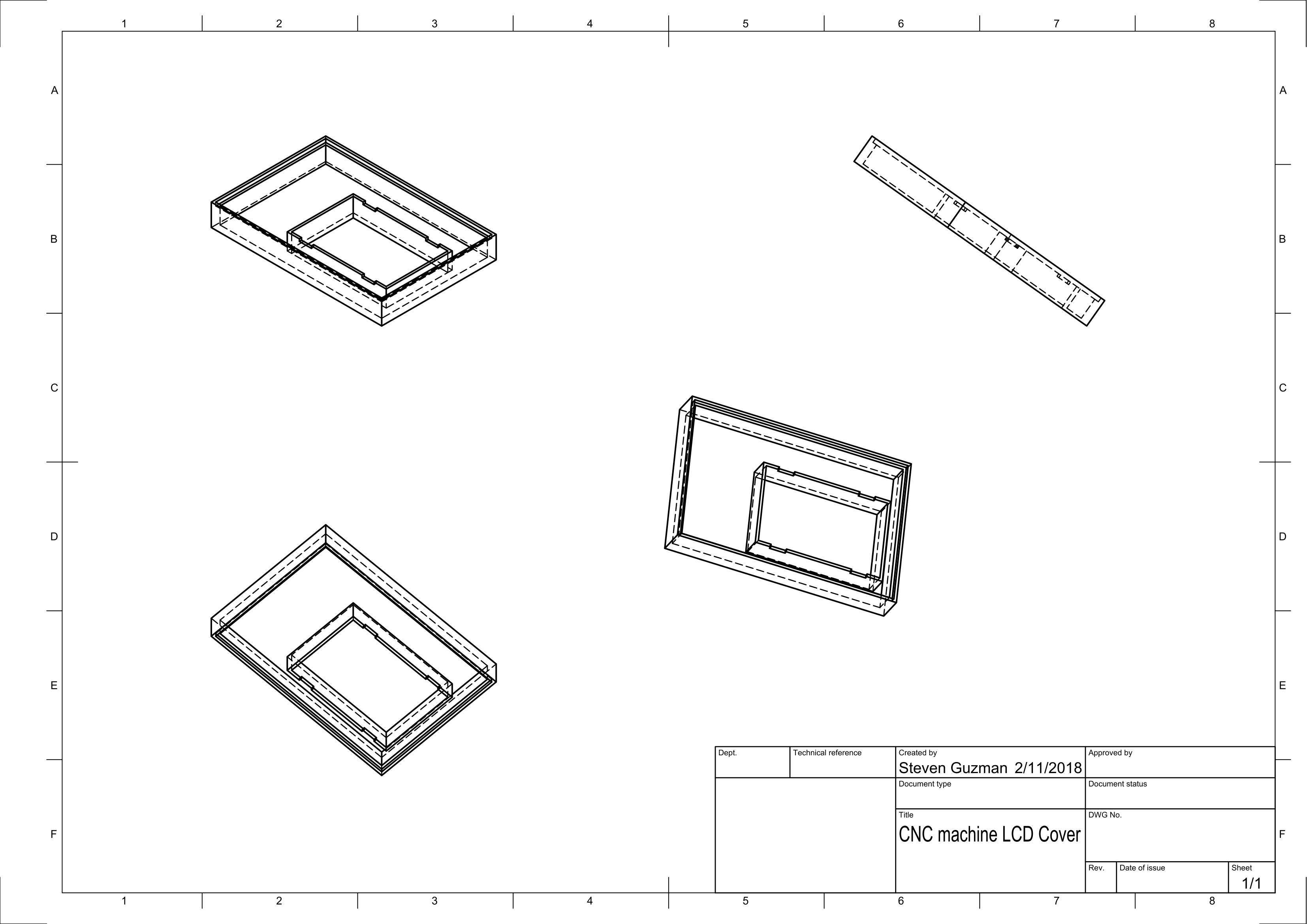
Now for the enclosure, I designed it using Fusion 360. Honestly, I am not a Mechanical engineer/Designer so this was my first attempt at designing something in a CAD software. Mine you its really just a box but Fusion 360 makes it really easy to design for someone who had no prior experience.
I designed this in two pieces:
The bottom portion of the enclosure:
The Lid for the enclosure:
For material used for making this enclosure, I used my Maker Select V2 3D printer with PETG filament for the temperature resistance and flexibility.
I will include the STL files so you guys can 3D print this yourself.
ASSEMBLY
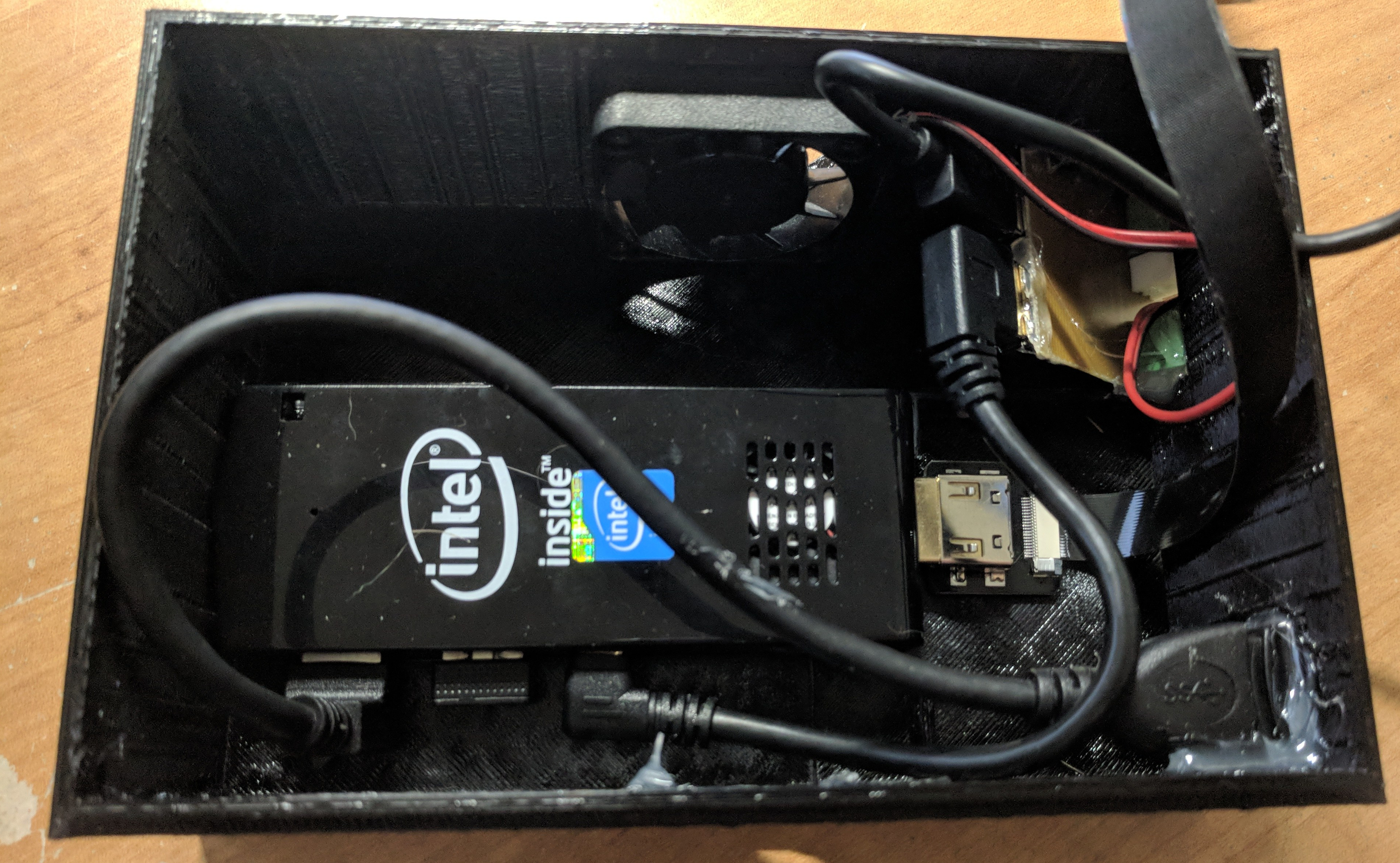
Now for the fun part, putting this thing together and hoping everything works without the magic white smoke lol jk. This was actually very easy to put together though there were a couple of design hick ups.
Image: 1
Image: 2
Image: 3
Image: 4
Image: 5
Since I wanted to get the print out as fast as possible, I sacrificed quality of the print which is why it looks the way it does but its very function.
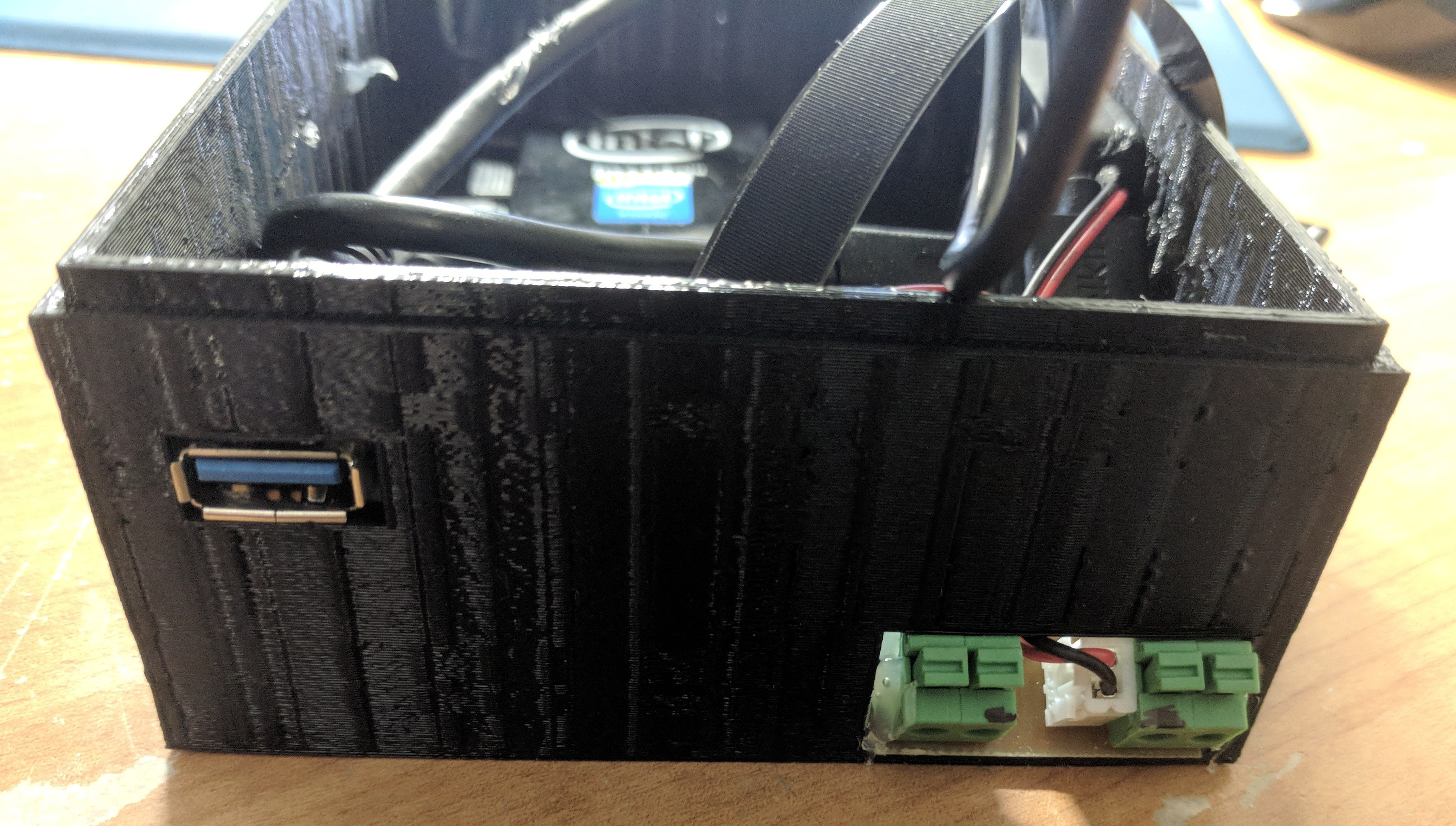
As I mentioned I did have some design issues after I was putting this thing together. If you look at image 3, you can see that the usb power board is tilted up and thats because I placed the cooling fan to close. The board was able to fit but I could not connect anything because the fan was blocking the connectors.
I decided to use hot glue to hold everything down because it wouldn’t be a DIY project if hot glue wasn’t involved.
In image 4, you can see I used some basic terminal block connectors to attach my 5V and 12V supply. You can also see the USB port to connect the arduino grbl controller board.
FINAL THOUGHTS/IMPROVEMENTS
Overall I enjoyed putting this project together. It’s made my project efficiency increase dramatically because I don’t have to take it out and set it up every time I want to make a board.
With anything we do, there’s always room for improvements. In a future version of this project I plan to improve the way I connect my external 5V and 12V supply instead of using the terminal blocks. I might possibly use some type of molex connector that can easily detach. To reduce the amount of external connectors, I could switch out the 12V fan with a 5V fan and run it with only one step down converter. I’m going to also move the fan placement so that I do not have to angle the usb power board.