
Its time to show you my 3.3V output boost Converter design. In one of my earlier post I showed you step by step on how to design your own boost converter and if you haven’t read that yet then click here.
You can purchase this board fully assembled by clicking here. 🙂
Lets get started:
Intro.
First of all, why do we even need this converter? Well every sensor, microcontroller, arduino, ESP8266, and various other digital components need a constant voltage. A constant voltage is necessary to maintain proper operation of these components.
Here we will see the advantage of this boost converter.
Specifications.
Below are the operating specs for this converter


- Note: Different Vin voltages gives you different max power output

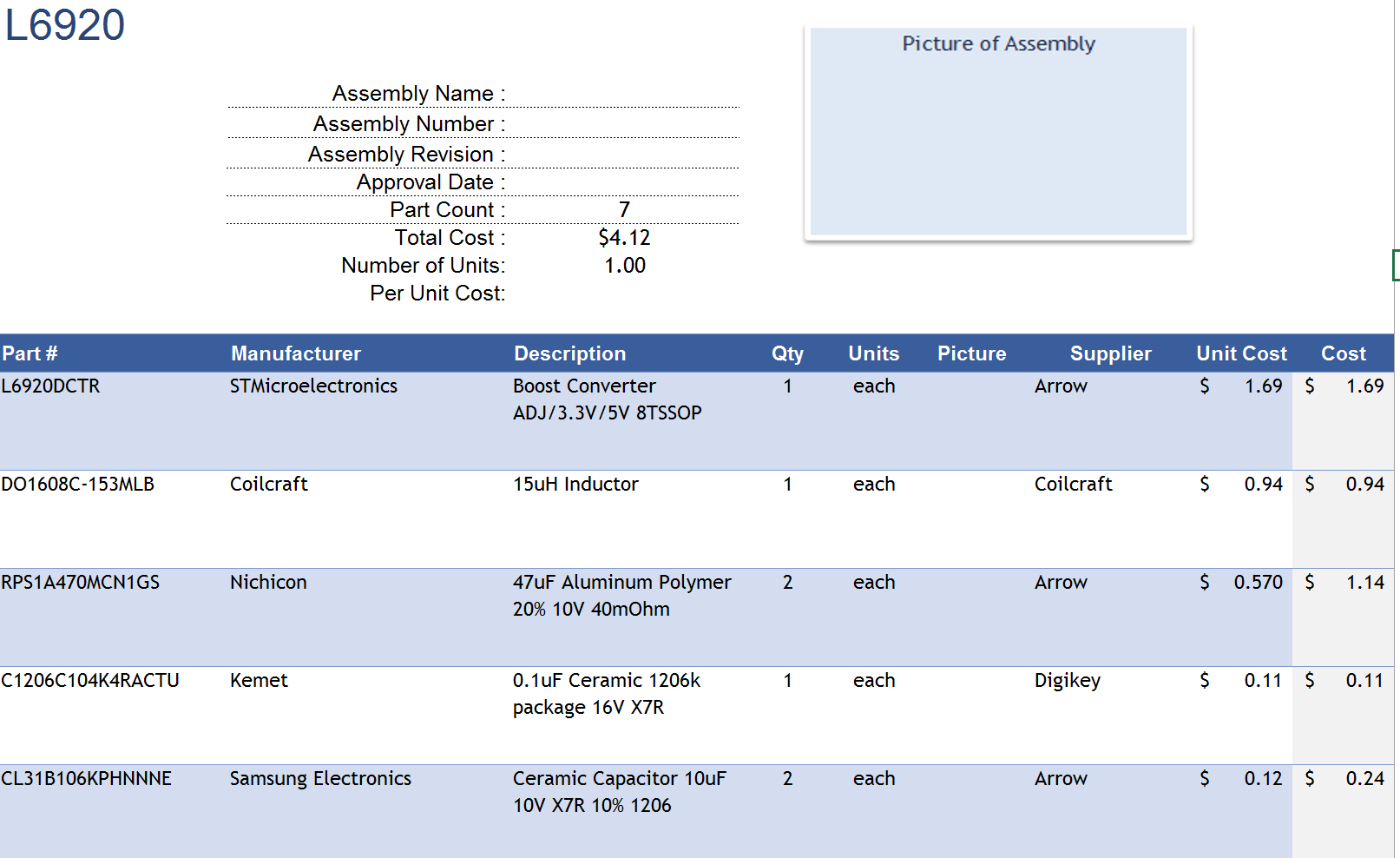
Bill of Materials.
Here is a screenshot of the bill of materials. I added the suppliers on the spreadsheet because I’ve found that some sites have better pricing than others.
Using octopart.com, you can actually find the best value for the component you’re looking for. I highly suggest you go look at the site.
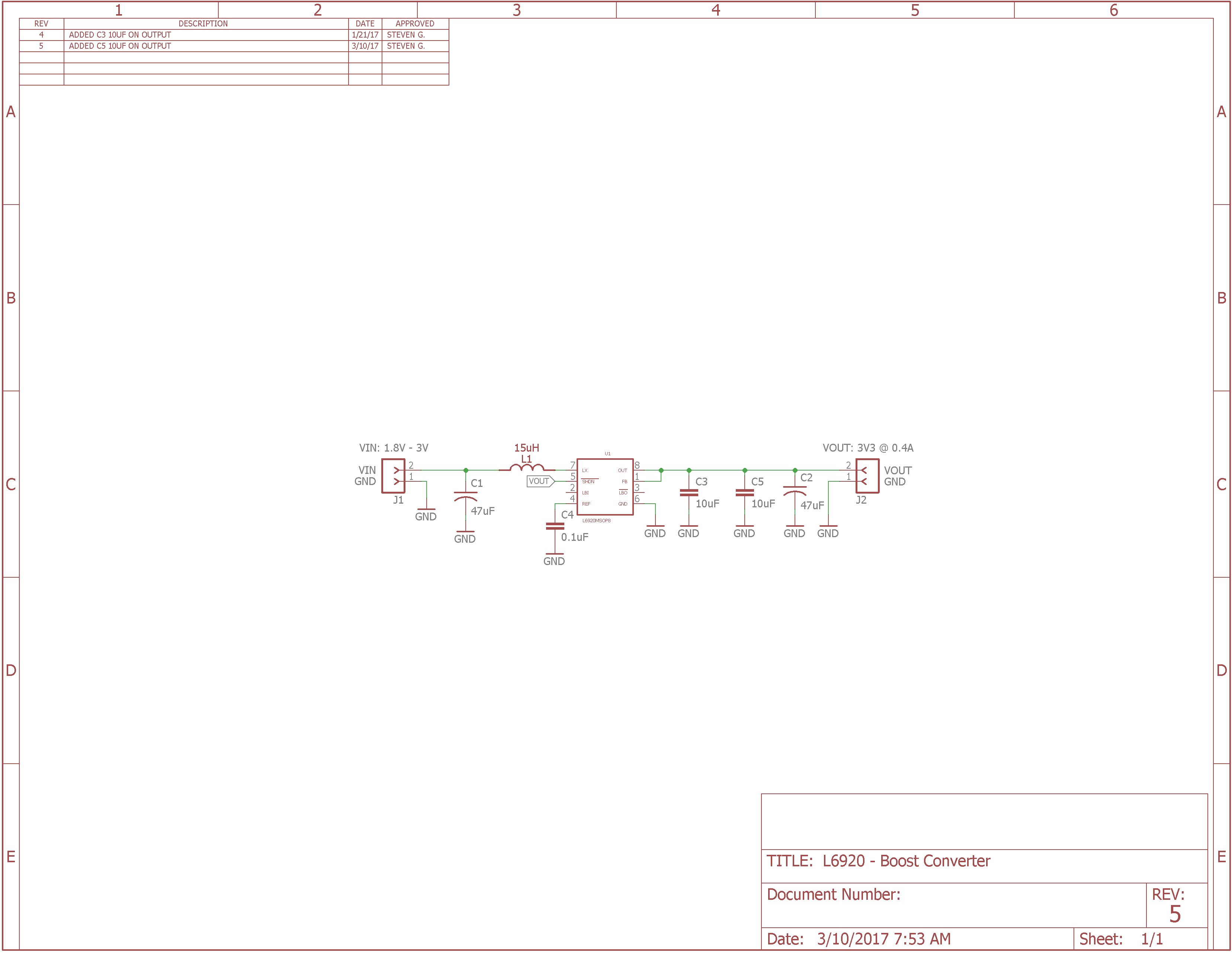
Schematic.
Attached here is the schematic for this project. All the original files are available for download at the bottom of the page.
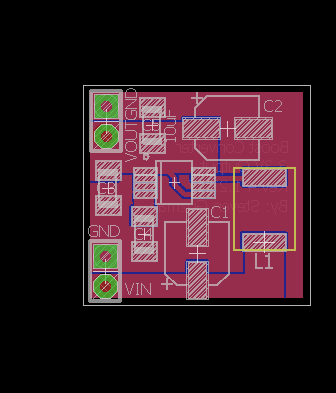
Layout.
I figure I’d help you guys out a bit if I added the layout for this board. My approach for this layout was to minimize the overall size in order to get a better price for manufacturing the board.
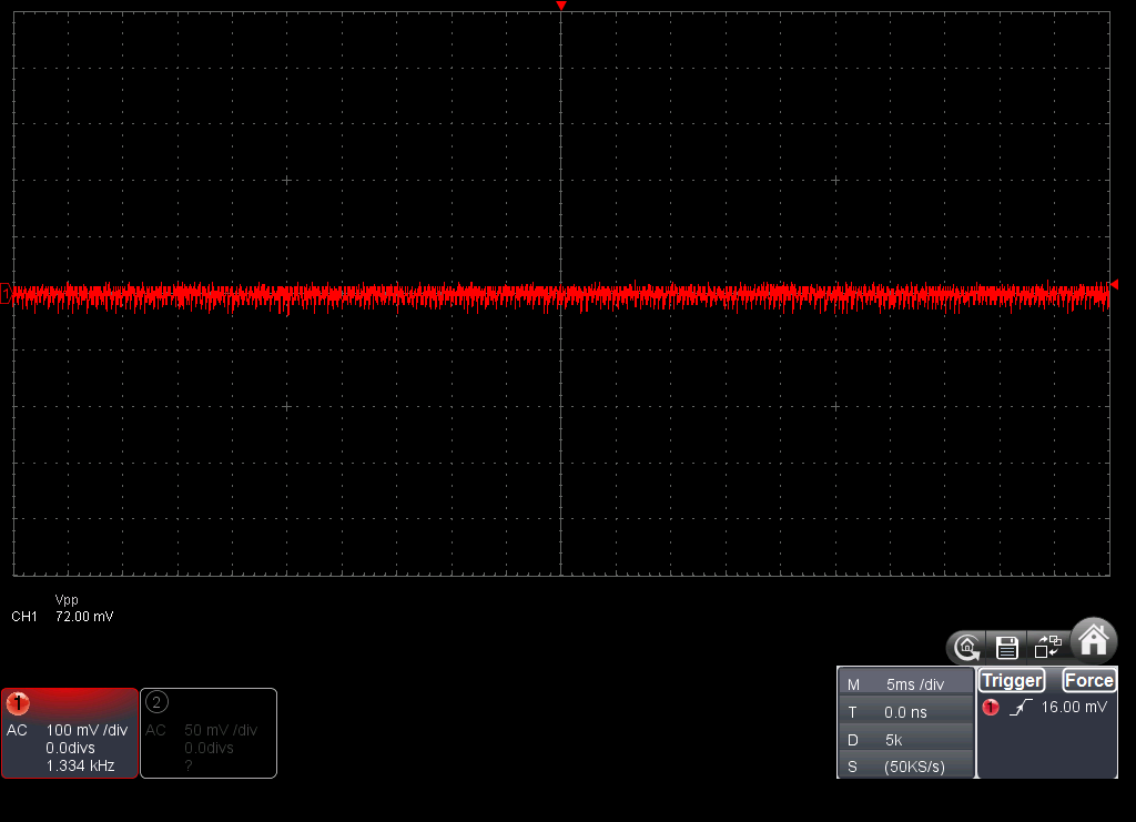
Testing.
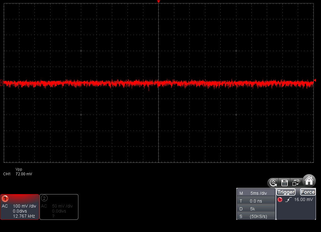
Here comes the fun part, actually testing what you designed. Now one thing that took me awhile to learn was that design and theory never really match reality. There are a lot of different parameters that are not accounted for when designing in theory.
A couple of the major issues that could make or break your design is parasitic elements. One of the biggest parasitic elements is ESR for output capacitors. This is the equivalent series resistance of the capacitor that is not taking into account when designing. In my post that covers the design of a boost converter, I emphasizes this topic to make you aware of this parasitic element.
Now, my design parameters consisted of loading the converter at 3 different voltage inputs (1.8V, 2.0V, and 2.4V). Each input voltage was loaded starting at 0.1A and ending at 0.4A. This load all depended on which input voltage was tested because the lower input voltage cannot provide the max output power.
First test – Vin: 1.8V @ 0.2A
Will add soon.
Next test – Vin: 2.0V @ 0.3A
Last test – Vin: 2.4V @ 0.4A
After completely the voltage ripple test, I also conducted a load regulation test at max load for each input voltage. I got a 1.5% voltage drop from calculated voltage meaning at full load, my output voltage was 3.25V at the lowest.
Downloads.

All files available here – Click


