Here is a new project I’m working on and hoping to get to a point where I can share the files and source code.
This is a replacement for a passive DC fuse box that you typically buy for low power solar projects.
This will allow you to remotely control 6 independent circuits each with a dedicated 25A max blade fuse. It uses an esp32 pico and each circuit has a 31A max current sensor. With the esp32, data logging can be incorporated and sent to influxDB server.
I’m very excited and hopefully I can get this project done so you can enjoy it as well
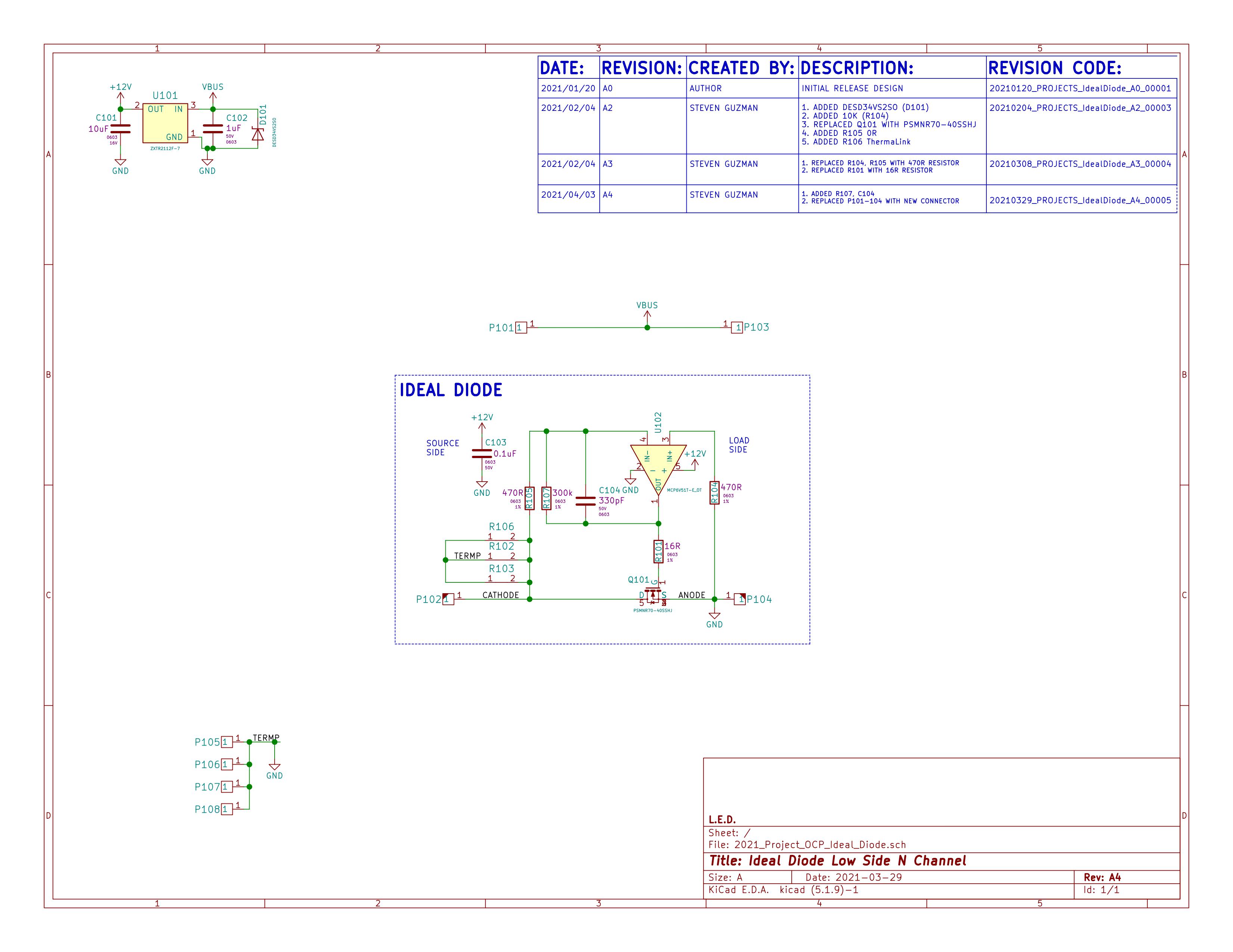
Replaced P102,P104 pads with high current part# 7460305
Added R107 (300k) and C104 (330pF) for better stability by lowering the gain
Update (All updates are already included in the github files, link at the end):
Updated R104, R105 to resistor value 470ohms for better reverse current protection threshold
Updated R101 to resistor value 16ohms for better stability
WHAT IS THIS?
What is an ideal diode? An ideal diode operates exactly as a traditional blocking diode that’s used to reverse current protection for a power path to protect the source from become the load and absorb power.
The only downside to using a diode is the power loss since most Shottky diodes, which is the a type of diode used primarily in power circuits, have a minimum voltage drop of 0.4V to allow current flow. This is an issue if you are trying to pass 50A through the diode which is a power loss of 10W which is a significant on design to eliminate that much heat from the diode.
The solution is to use is to use the ideal diode as a replacement for the Shottky diode. The ideal diode in summary is a linear op amp driving a mosfet with a low RDson internal resistance to turn on when current is flowing to the load and turn off when current tries to flow back to the source.
WHY DO WE NEED THIS?
Why is this circuit used and why is it needed?
The primary reason why I looked into this and designed this circuit was to have the ability to parallel multiple battery banks without having to worry if one of the banks ended up shorting out or having some fault that triggered the BMS system to turn off that particular bank.
This circuit is also known as an OR-ing diode because it allows the use of multiple parallel sources to help drive the load and the load alone. If one source has an issue then it can be removed without having to turn off the system to do so and in the case of a battery bank, it keeps it from either being charged from the other batteries in parallel in case of an over voltage condition and it keeps it from discharging to other banks in case of an under voltage condition.
HOW DO WE CREATE THIS?
How is this circuit made? Below I’ve created a discrete ideal diode using an op amp for driving and a Mosfet as the diode switch.
SPECIFICATION
Vinmin: 14V
Vinmax: 36V (This is limited by the mosfet and tvs diode, change those parts to increase input voltage range)
Imax: 30A ( This is dependent on the mosfet that is chosen, this rating is without a heatsink. I will perform test when I receive the actual boards as I used 2oz copper and should be able to handle more current without an issue. In theory this mosfet should be able to handle 400A with a proper heatsink)
SCHEMATIC
RENDERING
FRONT SIDE PCB
BACK SIDE PCB
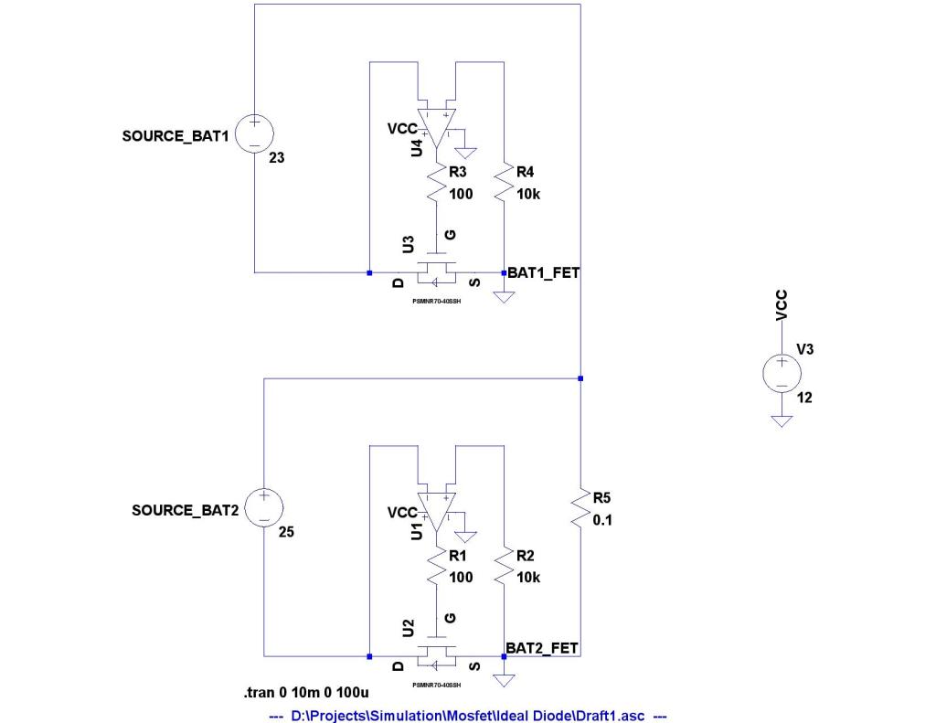
SIMULATION
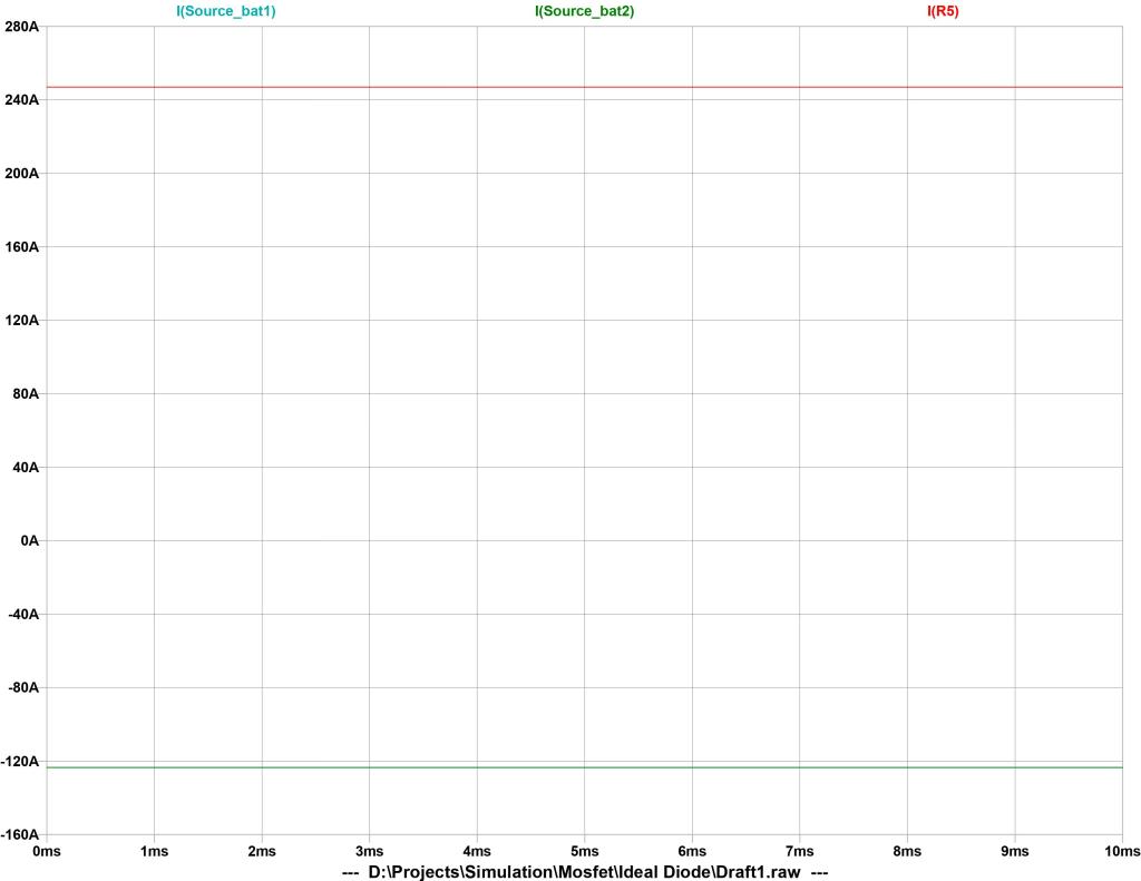
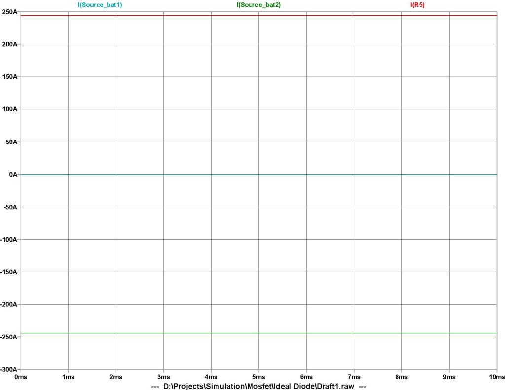
Below I also simulated the circuit and you can see what both the sources share the current when they are equal in voltage. But when source “BAT01” drops in voltage, which simulates either a faster discharge on that parallel cell or the bms turned off the battery pack due to a fault event, source “BAT02” is now providing all the current to the load. You can see that BAT01 ideal diode is blocking the current from charging the battery which is known as reverse current.
WHERECAN I DOWNLOAD THIS?
I’ve uploaded all the files, which included sources files and gerber, on my github below:
I strive to provide my content for free without using ads as I personally do not like ads in most website. If you can afford to donate anything via Paypal i would great appreciate it. Thanks:
INTRODUCTION:
This project was created in order to provide protection for my battery projects. I didn’t really trust the cheap low cost protection boards you find online so I decided to try and create my own.
The protection board I’ve designed has bidirectional current detection (can detect charging and discharging currents) which in turn means you can set independent OCP( over-current protection) for discharging current and charging current.
One thing to note before hand is that the current maximum current that can flow is about 5A due to lack of heatsink on the powerFETS. Adding heatsink is necessary to allow more current
Main features:
Over current protection with output latch open when tripped
Under voltage protection for the whole battery pack
Theoretically 45-50A pass-through current ( will require heatsink)
In the next sections I will discuss in more detail this project.
SPECIFICATIONS:
Here are some more technical details of this project
Minimum input voltage (V)
10
Maximum input voltage (V)
34
Maximum current (A)
50A*
Quiescent current (mA)
**
Undervoltage protection
Yes (adjustable)
Overcurrent protection
Yes (adjustable)
Short circuit protection
Yes***
Overvoltage protection
No
*Maximum current passing through this board will depend on sizing and adding a heatsink to the power mosfets
**Quiescent current has not been measured yet but it is below 1mA during normal operation with a 4S battery. This will change slightly when using more cells in series
***Theoretical the supervisor IC will latch when the overcurrent protection section detects its threshold. This will need testing to confirm
SCHEMATIC AND CIRCUIT DETAILS
Here in this section I will discuss the project in more detail by talking about the different sections used to create this whole circuit.
Lets first discuss the over-current/short-circuit protection sections of the circuit:
Bidirectional Current sensor
Here we have the heart of the over-current detection. We have the MAX4081FASA which is a bidirectional current sense IC that can handle a max VCC of 76V which is more than enough for our applications. The FASA has an internal gain of 5V/V coupled with a 10 milliohm sense resistor value ( I have two 20 milliohm in parallel for size reduction) this will allow the sense current of up to 50A.
REF1A is tied to 5V reference IC and REF1B to ground. With this we have a bias point of 2.5V meaning that when no current is passing the voltage on the OUTPUT pin 5 is 2.5V. When current is discharging into a load the output will rise up to 5V being the 50A max. When current is flowing the other direction to charge the batteries then it will go below 2.5V to 0V being 50A max.
In order to both detect charging and discharging current since I will be using this for a battery pack, I had to create a circuit that detects both an upper limit and lower limit. Hence I went with a window comparator to detect charge and discharge values.
Window comparator with latching supervisor IC
Here is where you can adjust your own over-current detection points for charging and discharging and they can be set independently from each other. The idea here is when the output from the max IC is within the window of the voltage values you set from the voltage divider values on pin 3 and pin 6, the output of the opamp will be high. As soon as the output value goes above or below those set points, it will pull the output of the op-amp low and trigger the supervisor IC.
The supervisor IC is very important because this is what controls the power mosfets allowing current to pass through. This one is different from normal supervisor ICs because when this triggers, the output is latched low and this pulls the power mosfets high causing them to stop current flow. The only way to clear the fault condition is to pull the clear pin 1 to 5V. What I have done is add the option for a push button on the board directly or pads to run the clear pin trigger somewhere else.
Here is a simple equation to calculate the discharge current detection resistor values on PIN3 of the op amp:
(0.05 V/A * X) + 2.5V = VdetectHigher ; X = current trigger desired
For charging current detection here is the equation for the lower voltage detection of the op amp PIN 6
(0.05 V/A * X) – 2.5V = Vdetectlower; X = current trigger desired
Here is the power mosfets controlled by the supervisor IC. When no fault condition is triggered then the supervisor IC pulls Q4 to high causing the 10k resistor to be tied to ground. This then creates a voltage difference between the gate and source for the powerFETS allowing current to flow. When an overcurrent fault condition is triggered the supervisor IC is then pulled low and Q4 stops conducting which in turns unties the 10k resistor from ground and makes the gate and source the same potential.
Now the under-voltage protection scheme works by using a different supervisor IC measuring the input voltage. When the voltage falls below the threshold then the output pulls low and stops current flow in the powerFET
Here you see this circuit in action. A voltage divider is used to bring down the input voltage of the pack to a range the supervisor can handle. I have defined some voltage divider resistor values for different size battery packs in which it will trigger when the threshold is hit. I only used one MOSFET for this because this will stop discharging current but will allow charging current to flow via the body diode until the input voltage is above the threshold and then turn on the mosfet.
Here you have to take some precautions not to kill the mosfet when an event triggers an under-voltage event and you try to charge the pack.
When an event happens, start charging the pack with 0.5A-1A until there is about 1V above the under-voltage value. Then maximum current charging can be applied. This part of the circuit will need more tweaking in the future
CONCLUSION / IMPROVEMENTS
Hopefully this project will help someone out. I created this to help protect my batteries and to allow the flexibility to adjust as much values as I can and have as much control of my protection circuitry as possible. Of course this is not perfect and I am still working on improvements.
IMPROVEMENTS:
Figure out a way to protect Under-voltage powerFET from getting damaged when charging through the body diode initially until the supervisor IC allows current to flow through the FET and not the body diode
Use DPAK powerFETS instead of IPAK due to cost. Size increase is negligible or non-existent
Create a heatsink to provide maximum current discharge through mosfets. Currently the maximum current discharge without heatsink is roughly 5A without getting too hot. Will do testing after its completed.
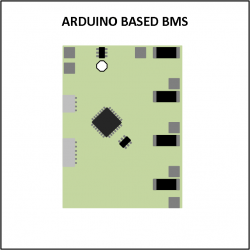
This is an updated post regarding my 4S arduino based lithium ion balance management system (BMS).
If you click here, you will see the original post with details on the project.
IMPORTANT CHANGES:
Replaced external voltage reference to a more stable one. Upgraded to a REF3012AIDBZT from Texas instrument. This does not require an output capacitor for stability.
Modified Buck converter RT6208GE. Grounded pin 4 to set the max peak current to 50mA which is an average current of 25mA. This was done to eliminate audible oscillation from the buck converter
Increased copper traces for ADC pins A0-A3
Better layout to increase continuous copper plane on internal layer
updated 01/13/2019: For the new arduino version, load bootloader with 8MHz clock. I did more testing and this was more stable and accurate on the adc then the 1MHz clock setting.
I will be doing testing on these new versions and see how they perform. I will post results as soon as I can. Also below I will attach all files needed (schematics, gerber, bom) if you wish to make your own.
Now this might seem like it was a complete waste of time to try and reinvent the wheel with creating my owm custom BMS solution. You can buy them on ebay or alibaba or banggood for super cheap and it seems like a plug and play solution.
One problem I see with this, at least for me, is that I dont completely trust those cheap BMS system. I like to buy something that is reasonable as well as trusting that it will safely protect my cells from unbalancing. Another this is that I like to have flexibility with how I balance my cells or anything else.
Now this is where the custom arduino BMS came into play. I’ve designed this bms to handle a 4S battery pack so upto 16.8V fully charged and 14.8V nominal. The balance discharge current can be adjusted by simply replacing the discharge resistor with any value you wish. Just to add this does not have over current or over voltage protection..yet 🙂 I’m currently working on an add on for this so stay tuned for that future update.
Lets get started with all the cool details for this arduino bms.
3D RENDERING
Here i just wanted to show you the 3D rendering images of the final board. The rendering was created using kicad and its pretty nice actually for an EE cad software.
The heart of this system is the atmega328P running the minicore arduino bootloader[1]. From here you have the 4 balancing passive resistors to the right of the board. The best part of this project is that you can replace these resistors to any value you want to customize the balance current.
The one thing that this does not have is overvoltage and overcurrent protection but that will be a separate circuit later on ;).
Now we can talk about the main features below in the schematic section.
SCHEMATICS
Below are images of the full schematics for this project:
The first page of the schematic files is a hierarchy block level of the system to help understand how a lot of these subcircuits are linked together. Below I’ll breakdown all the pages and what exactly they do.
1. Hierarchy Block:
This is the overview block level that links the subcircuits on the separate pages. I normally like to design my projects this way if I have more than 2 subcircuits because its easier to see how things are working together
2. Power Supply
This section is just the power supply section to power the arduino. This is a high differential buck converter. The input voltage can go up to 36V and output down to 1.8V with an active quiescent current of only 190uA. Now the most important part is the quiescent current because we are trying to eliminate any wasted current since this is for a battery operated system and we do not want to drain the batteries faster than needed.
3. MCU
The MCU page has the Atmega328P and all the corresponding IO related to it. Im using A0-A3 to measure the batteries via a resistor divider
This page also includes the external reference voltage used instead of the built in 1.1V from the atmega328p. Its a 1.25V external voltage reference that has a better tolerance at a range of temperatures.
4. Balancing Circuit
This page has the balacing circuit which is incharge of discharging the battery cell that has a higher potentional. The heart of this is a bidirectional N-channel mosfet that allows current to flow in both directional either during discharge or during charging.
5. Connectors
This page has the power pin connectors and the BMS pads that connectors to the lithium cells.
Now that we’ve gone through the schematic lets go into the second most important part and that is the arduino code.
ARDUINO CODE
Now probably the second most important part is the arduino code that will control the mosfets triggering the discharge when a preset voltage difference is hit.
#include "Adafruit_SSD1306.h"
/* Revision: A9
* Written by: Steven Guzman
* Date: 7/10/2018
* Description: This is a customizable BMS system for a 4
* cell lithium ion pack.
*/
#include "Wire.h"
#include "avr/wdt.h"
#define OLED_RESET 4
Adafruit_SSD1306 display(OLED_RESET);
#define NUMFLAKES 10
#define XPOS 0
#define YPOS 1
#define DELTAY 2
//////////////////////////////////////////////
// This variable is used for checking on
// whether the OLED screen is attached or not
//////////////////////////////////////////////
int check = LOW;
//////////////////////////////////////////////
// Sampling number for analog read values.
// Will use this sample size to calculate a
// better estimation of the analog value
//////////////////////////////////////////////
int samples = 100;
//////////////////////////////////////////////
// This is the max difference that the cells
// can achieve in respect to each other
//////////////////////////////////////////////
float tol = 0.03;
//////////////////////////////////////////////
// To temporaly store analog values from the
// cell voltages to average out later with
// the number of samples taken
//////////////////////////////////////////////
float temp_cell[4];
//////////////////////////////////////////////
// Float array to store unconverted cell values
//////////////////////////////////////////////
float cell[4];
//////////////////////////////////////////////
// Variable array to store converted voltage
// values for cell measurement
//////////////////////////////////////////////
float B[4];
//////////////////////////////////////////////
// Variable array to store voltage differences
// between cells
//////////////////////////////////////////////
float diff[4];
/////////////////////////////////////////////////
// Variable used for digital output
// signals
/////////////////////////////////////////////////
int BAT[4];
/////////////////////////////////////////////////
// Variable used for storing the cell pack
/////////////////////////////////////////////////
float PACK = 0.000;
/////////////////////////////////////////////////
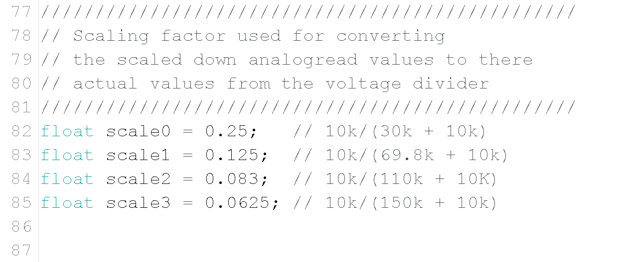
// Scaling factor used for converting
// the scaled down analogread values to there
// actual values from the voltage divider
/////////////////////////////////////////////////
float scale0 = 0.25; // 10k/(30k + 10k)
float scale1 = 0.125; // 10k/(69.8k + 10k)
float scale2 = 0.083; // 10k/(110k + 10K)
float scale3 = 0.0625; // 10k/(150k + 10k)
#if (SSD1306_LCDHEIGHT != 32)
#error("Height incorrect, please fix Adafruit_SSD1306.h!");
#endif
void setup()
{
Serial.begin(9600);
analogReference(EXTERNAL); // Configure reference voltage for
// external 1.25V
//////////////////////////////////////////////
// After switching to external reference you
// need to read a value a couple times before
// the reference has stabalized.
//////////////////////////////////////////////
analogRead(A0);
analogRead(A0);
analogRead(A0);
delay(20);
// Setup up watchdog timer to reset
// after 4 seconds
wdt_enable(WDTO_4S);
///////////////////////////////////////////////
// Variables to set the digital output
// pins 1-4
///////////////////////////////////////////////
BAT[0] = 5;
BAT[1] = 6;
BAT[2] = 7;
BAT[3] = 8;
///////////////////////////////////////////////
// Setting digital pins to output configuration
///////////////////////////////////////////////
pinMode(BAT[0], OUTPUT);
pinMode(BAT[1], OUTPUT);
pinMode(BAT[2], OUTPUT);
pinMode(BAT[3], OUTPUT);
///////////////////////////////////////////////
// Sets the digital outputs to an initial low
// state
///////////////////////////////////////////////
digitalWrite(BAT[0],LOW);
digitalWrite(BAT[1],LOW);
digitalWrite(BAT[2],LOW);
digitalWrite(BAT[3],LOW);
}
void loop()
{
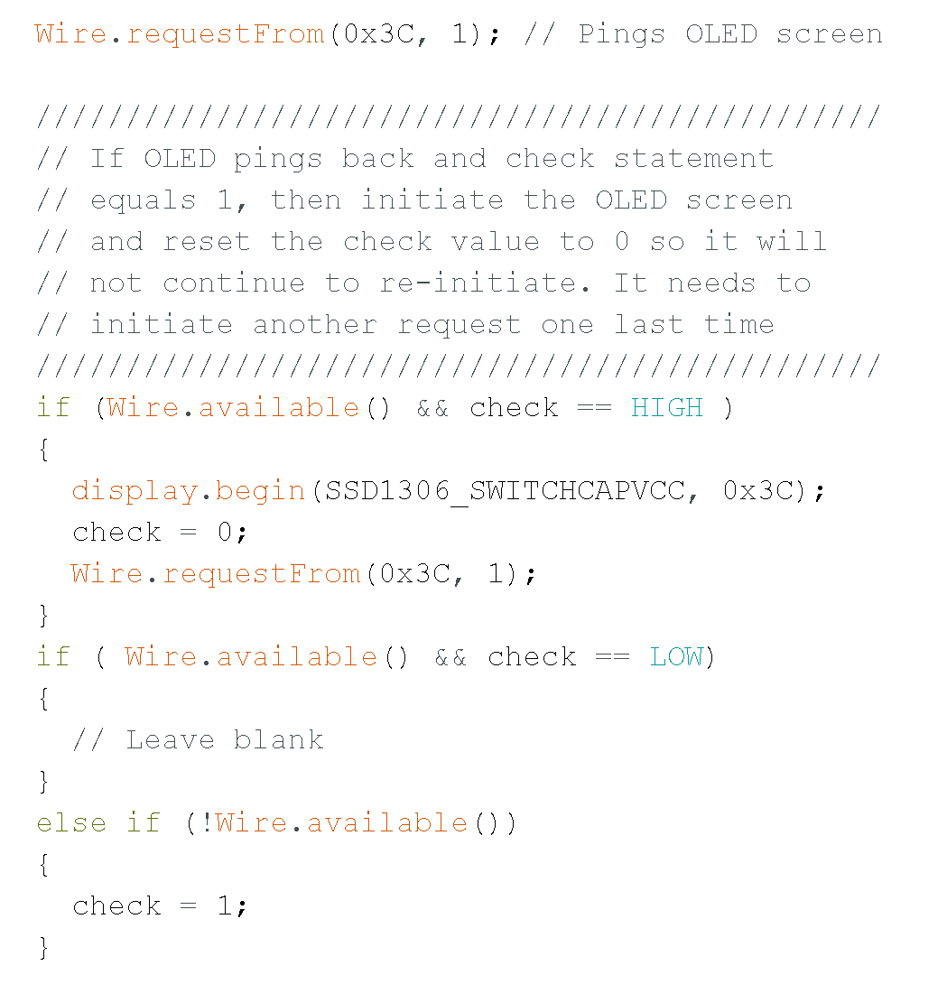
Wire.requestFrom(0x3C, 1); // Pings OLED screen
///////////////////////////////////////////////
// If OLED pings back and check statement
// equals 1, then initiate the OLED screen
// and reset the check value to 0 so it will
// not continue to re-initiate. It needs to
// initiate another request one last time
///////////////////////////////////////////////
if (Wire.available() && check == HIGH )
{
display.begin(SSD1306_SWITCHCAPVCC, 0x3C);
check = 0;
Wire.requestFrom(0x3C, 1);
}
if ( Wire.available() && check == LOW)
{
// Leave blank
}
else if (!Wire.available())
{
check = 1;
}
///////////////////////////////////////////////
// Sets the temp variable array back to zero
///////////////////////////////////////////////
for (int x = 0; x <4; x++)
{
temp_cell[x] = 0.00;
diff[x] = 0.00;
cell[x] = 0.00;
}
///////////////////////////////////////////////
// For loop used to record battery cell voltage
// information and used later to average out
// the readings
///////////////////////////////////////////////
delay(100);
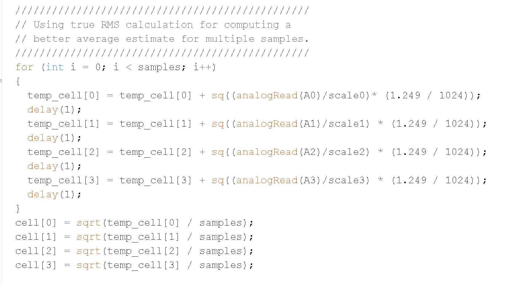
////////////////////////////////////////////////
// Using true RMS calculation for computing a
// better average estimate for multiple samples.
////////////////////////////////////////////////
for (int i = 0; i < samples; i++)
{
temp_cell[0] = temp_cell[0] + sq((analogRead(A0)/scale0)* (1.249 / 1024));
delay(1);
temp_cell[1] = temp_cell[1] + sq((analogRead(A1)/scale1) * (1.249 / 1024));
delay(1);
temp_cell[2] = temp_cell[2] + sq((analogRead(A2)/scale2) * (1.249 / 1024));
delay(1);
temp_cell[3] = temp_cell[3] + sq((analogRead(A3)/scale3) * (1.249 / 1024));
delay(1);
}
cell[0] = sqrt(temp_cell[0] / samples);
cell[1] = sqrt(temp_cell[1] / samples);
cell[2] = sqrt(temp_cell[2] / samples);
cell[3] = sqrt(temp_cell[3] / samples);
////////////////////////////////////////////////
// Scale up the cell values and then convert to
// to voltage values
////////////////////////////////////////////////
B[0] = (cell[0]);
B[1] = ((cell[1] - cell[0]));
B[2] = ((cell[2] - cell[1] ));
B[3] = ((cell[3] - cell[2] ));
PACK = B[3] + B[2] + B[1] + B[0];
///////////////////////////////////////////////////////////////////
// Compares each cell voltage to each other and then finds the
// lowest cell value. Then it stores the difference between the
// lowest cell and the remaining cells for comparison
///////////////////////////////////////////////////////////////////
if ( (B[0] <= B[1]) && (B[0] <= B[2]) && (B[0] <= B[3]))
{
diff[1] = B[1] - B[0];
diff[2] = B[2] - B[0];
diff[3] = B[3] - B[0];
}
else if ((B[1] <= B[0]) && (B[1] <= B[2]) && (B[1] <= B[3]))
{
diff[0] = B[0] - B[1];
diff[2] = B[2] - B[1];
diff[3] = B[3] - B[1];
}
else if ((B[2] <= B[0]) && (B[2] <= B[1]) && (B[2] <= B[3]))
{
diff[0] = B[0] - B[2];
diff[1] = B[1] - B[2];
diff[3] = B[3] - B[2];
}
else
{
diff[0] = B[0] - B[3];
diff[1] = B[1] - B[3];
diff[2] = B[2] - B[3];
}
//////////////////////////////////////////////////////////////////
// It enables the balancing protocol for a given cell that has a
// greater voltage difference from the lowest cell and the set
// tolerance.
//////////////////////////////////////////////////////////////////
delay(1);
for ( int x = 0; x tol )
{
digitalWrite(BAT[x], HIGH);
delay(1);
}
else
{
digitalWrite(BAT[x], LOW);
delay(1);
}
delay(1);
}
// text display tests
display.setTextSize(1);
display.setTextColor(WHITE);
display.setCursor(0,0);
display.print("V1:");
display.print(B[0]);
display.println("V");
display.print("V2:");
display.print(B[1]);
display.println("V");
display.print("V3:");
display.print(B[2]);
display.println("V");
display.print("V4:");
display.print(B[3]);
display.println("V");
display.setCursor(70,0);
display.print("VP:");
display.print(PACK);
display.print("V");
display.setCursor(70,8);
display.print("Config:");
display.print("4S");
display.display();
delay(1);
display.clearDisplay();
wdt_reset();
}
Lets break down this code in order to understand my thought process behind this.
The samples variable is used to create an average sampling of the battery cells to eliminate any noise issues. The averaging technique I used in this project is a little different than most but I will explain later on
The next variable is the tol variable. This variable is the maximum voltage different between the lowest cell and the rest of the cells in the 4S pack. Currently its set to a maximum of 30mV difference but this can be set to a minimum of 10mV because of the 8-bit adc on the arduino.
Here is the scaling factor for the adc from the cell measurements. We have different values because in order to get the best accuracy measuring in reference to ground, different values were needed for measuring cell 1 which has a max of 4.2V and cell 4 which measures a max of 16.8V.
This portion of the code is mainly for the OLED screen. It allows for the screen to be removed and re attached without having to reset the arduino. Before you had to initialize it in the setup but with this loop it is initialized in the main loop when it detects the screen.
Now this section is averaging the adc values from all 4 cells to get a best measurement of the cell voltage values. Instead of using the traditional sample 25 and take the average, I’m using a true RMS calculation that will give you a slightly better voltage measurement that just taking the average. It will be at a closer measurement to your multimeter than using average sample.
CONCLUSION / ISSUES
Here is the final PCB:
I’m pretty excited to do more testing on this and I will post my technical review later on that includes current consumption, maybe a mini manual on how to use it or change values for your own build.
Again this does not include an over voltage or over current protection circuit but I decided to make that a separate board with its own controller in order to make the board as small as I could and isolate the two circuits as a redundancy. I’m still making some tweaks and might make another revision but all in all I’m very happy about it.
Some current issues that I know off.
You might have to calibrate with a known good multimeter. The arduinos ADC has some weird issues with analogPin A2 measuring higher than the rest. I added a calibration value in the code to help with that.
With the Arduino mini, there is a need for a USB to UART controller to upload your sketches and this could also be used for the ESP8266.
This project is inspired and based off the Sparkfun’s FT231X breakout board design. I’ve created this project because 1. I like designing and soldering electronics 2. Try to create a cheaper alternative to the popular FT232RL and also add 1 or 2 features to the current FT231X breakout board.
BILL OF MATERIALS
For the bill of materials, its pretty straight forward. I’ve attached links to digikey for each component as I find them easier to order from but you could also get the parts from arrow or mouser as well.
Below I’ve attached an image of the schematic but i’ve also attached the original kicad files and a PDF version of the schematic at the end of the post.
OSHPARK
If you feel like you want to get this board made, I’ve attached a link to my oshpark project. With oshpark, I find they make great quality boards at a great price for small sized boards.
FINAL THOUGHTS
I know this was a short post and project but I found it important to share another option for those’s who want to find a cheaper solution and want to learn along the way. You can find a lot cheaper solutions on amazon that are china made but i’ve read stories in some cases that they were not genuine FT232RL ICs. If you wish to build your own, its very easy and rewarding at the same time.
In the next revision I will add LEDS for TX and RX indication as for this version I eliminated to save some cost and space.
Arduino and the implementation of GRBL has allow for amazing things to be created. One of those things are low cost CNC machines that enable us to create anything we want.
I bought myself a low cost CNC engraver from amazon and after modifying it, it has been one of my best investments because as en electrical engineer I can create PCB boards to test my designs here at home and verify before getting them sent out. One problem I usually have is that I use my laptop to run the gcode software and my laptop is really big and sometimes a hassle to keep on my desk.
My solution was to create this project and make a standalone CNC machine controller to run the gcode software in a compact package. I tried fiddling around with using a raspberry pi 2 as my main PC but I’m still a beginner with raspberry pi’s and I had issues getting the settings right. My next option was to use a windows based machine and luckily I found just the solution.
In this tutorial I will explain how I put this together and what improvements could be made.
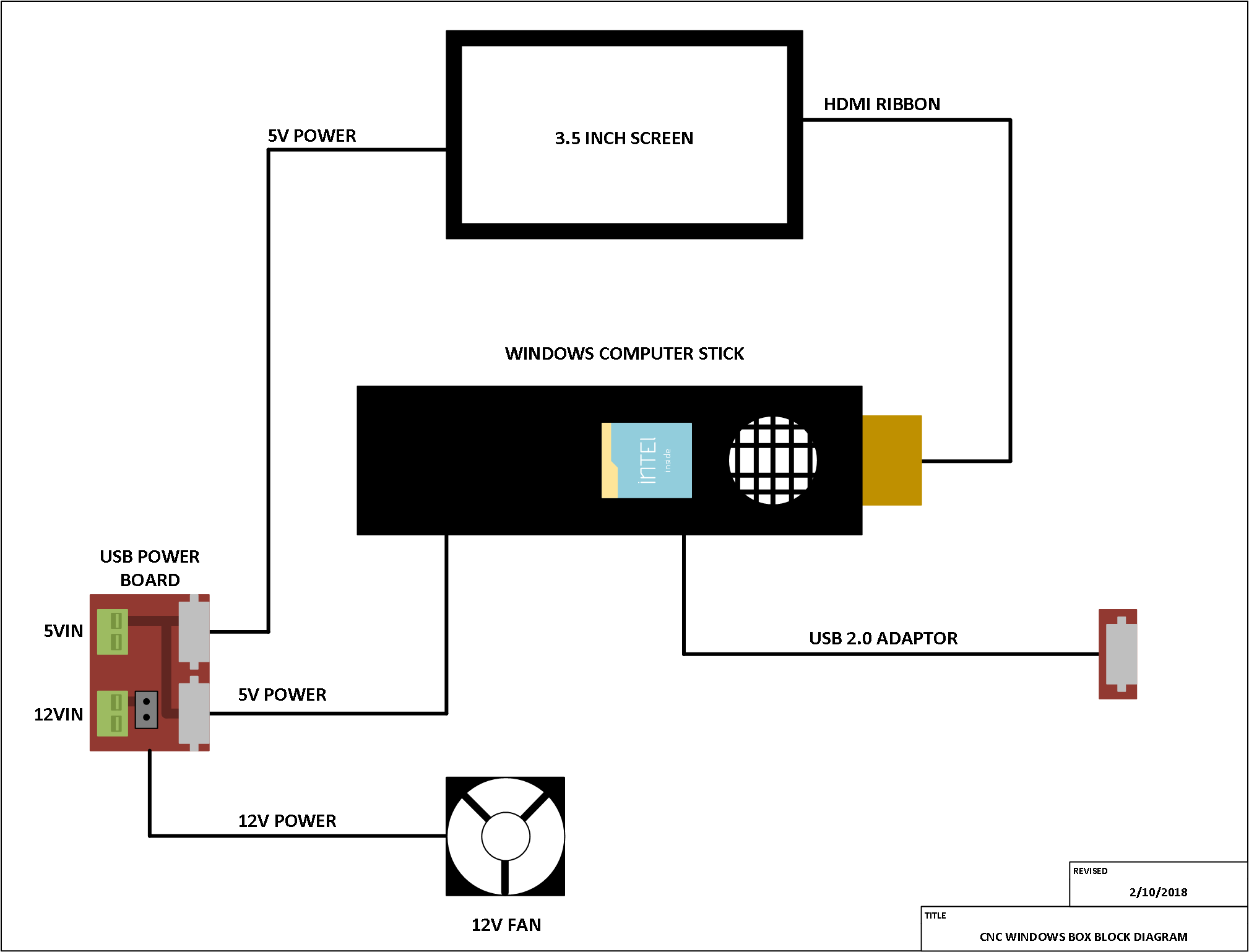
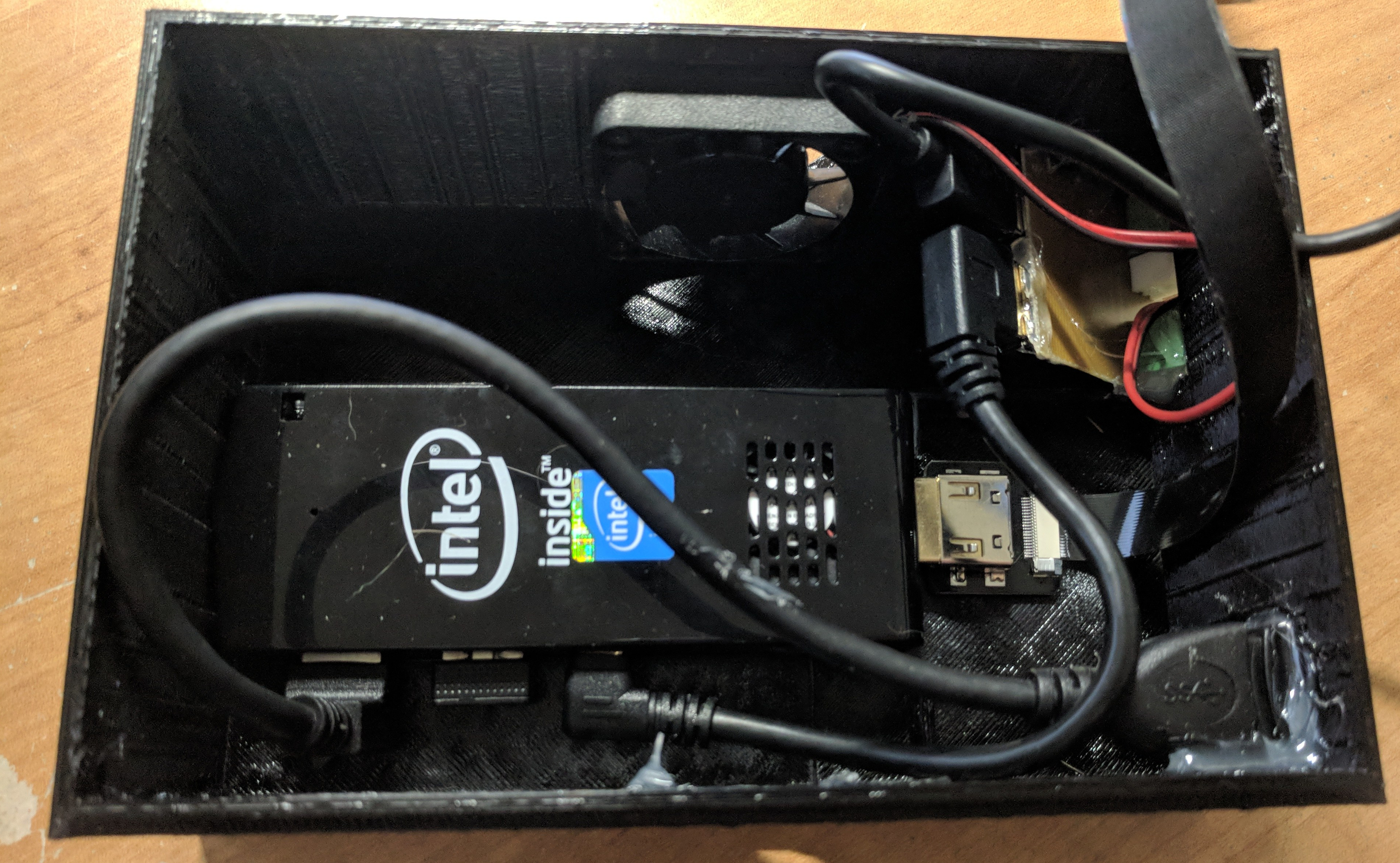
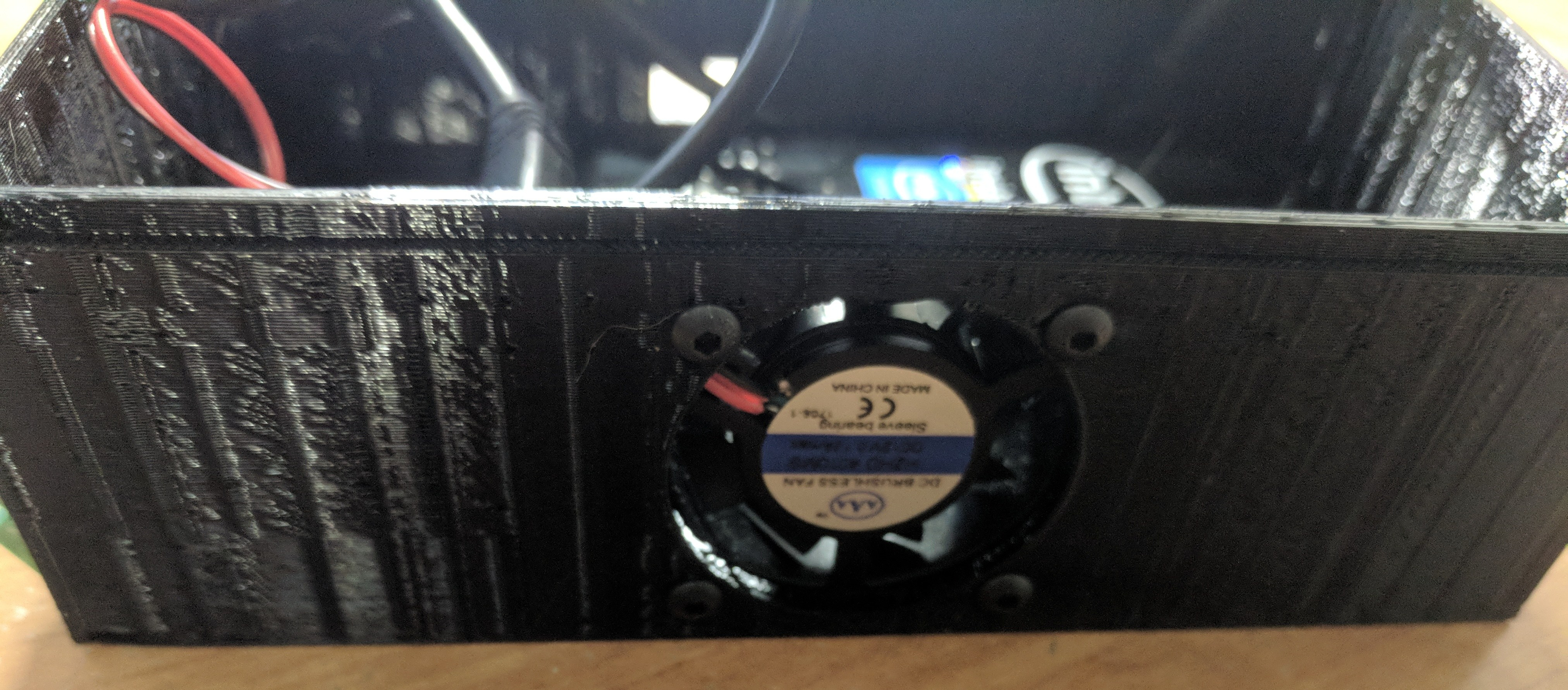
Here is the block diagram for how this project is wired. With the exception of the enclosure itself and the usb power board, everything was bought ready to go. I’ve added a fan as a just in case because the computer stick does generate some heat so the fan will prevent the system from over heating but so far it does not seem to be an issue with heat and therefore is an option.
The 5V and 12V supply are coming from my 24V power supply that powers my Arduino GRBL shield. What I did was use two step down converters 1) For 5V step down and 2) For 12V step down. I realized this might not be idle but it is my first revision of this project.
SCHEMATICS/ CAD DESIGN
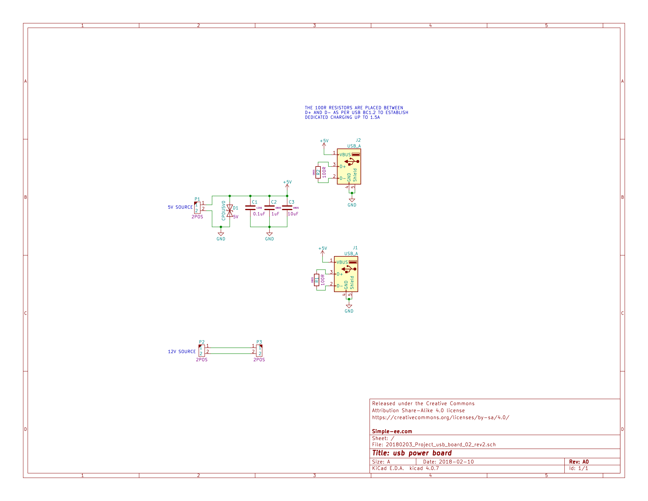
The only schematics I have is for the USB power board and I created that using Kicad. The board was basic, since both the screen and the windows computer stick ran on 5V via micro USB, I needed to distribute power from one source into two loads. To add some safety, I did add a TVS 5VWM diode to prevent over voltage spikes from destroying the devices along with some filtering capacitors.
If its a little blurry don’t worry because all original files will be included in a download link at the end.
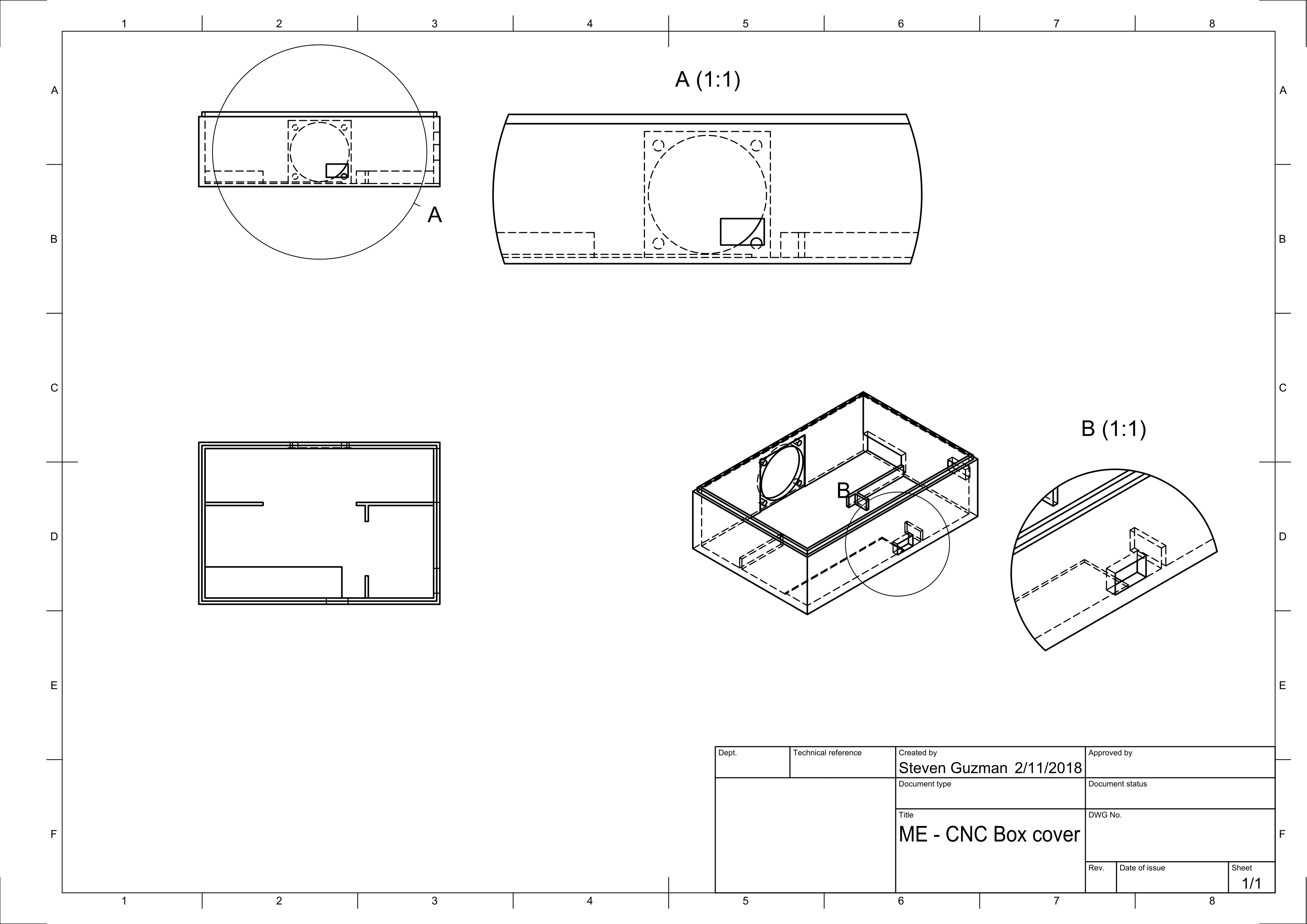
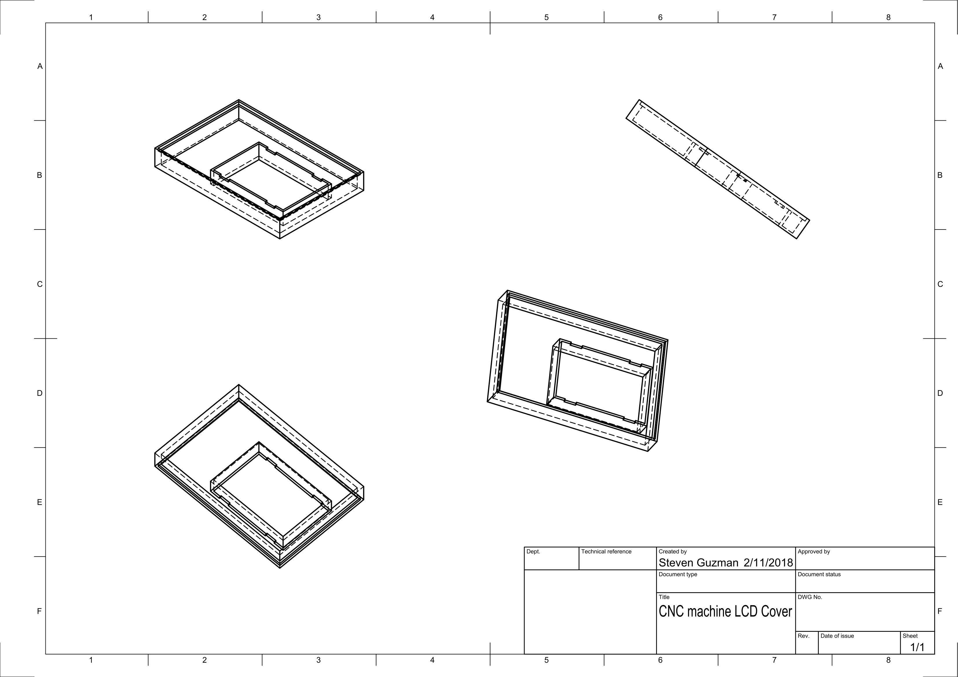
Now for the enclosure, I designed it using Fusion 360. Honestly, I am not a Mechanical engineer/Designer so this was my first attempt at designing something in a CAD software. Mine you its really just a box but Fusion 360 makes it really easy to design for someone who had no prior experience.
I designed this in two pieces:
The bottom portion of the enclosure:
The Lid for the enclosure:
For material used for making this enclosure, I used my Maker Select V2 3D printer with PETG filament for the temperature resistance and flexibility.
I will include the STL files so you guys can 3D print this yourself.
ASSEMBLY
Now for the fun part, putting this thing together and hoping everything works without the magic white smoke lol jk. This was actually very easy to put together though there were a couple of design hick ups.
Image: 1
Image: 2
Image: 3
Image: 4
Image: 5
Since I wanted to get the print out as fast as possible, I sacrificed quality of the print which is why it looks the way it does but its very function.
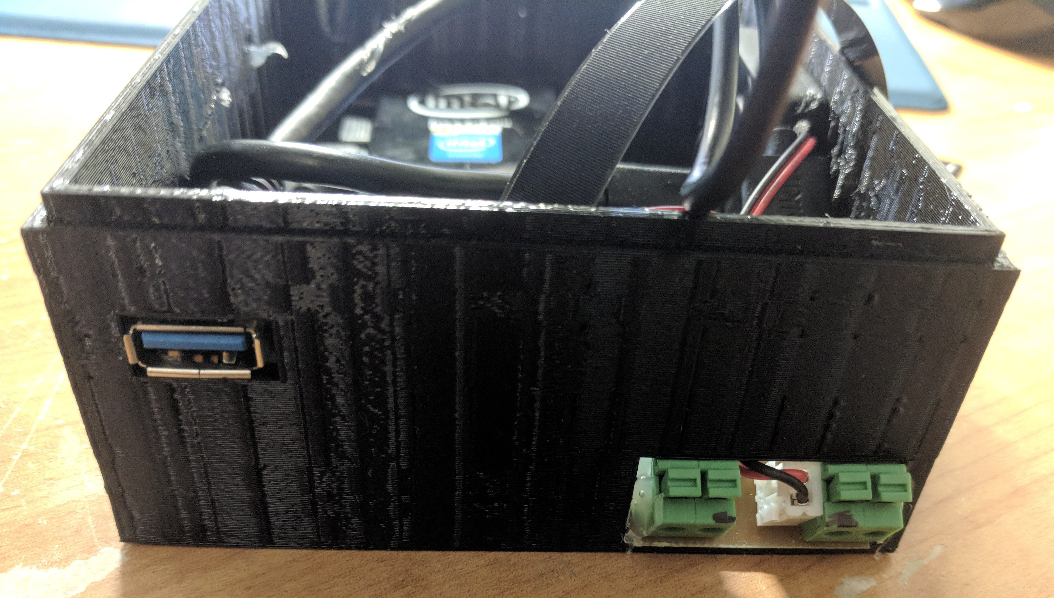
As I mentioned I did have some design issues after I was putting this thing together. If you look at image 3, you can see that the usb power board is tilted up and thats because I placed the cooling fan to close. The board was able to fit but I could not connect anything because the fan was blocking the connectors.
I decided to use hot glue to hold everything down because it wouldn’t be a DIY project if hot glue wasn’t involved.
In image 4, you can see I used some basic terminal block connectors to attach my 5V and 12V supply. You can also see the USB port to connect the arduino grbl controller board.
FINAL THOUGHTS/IMPROVEMENTS
Overall I enjoyed putting this project together. It’s made my project efficiency increase dramatically because I don’t have to take it out and set it up every time I want to make a board.
With anything we do, there’s always room for improvements. In a future version of this project I plan to improve the way I connect my external 5V and 12V supply instead of using the terminal blocks. I might possibly use some type of molex connector that can easily detach. To reduce the amount of external connectors, I could switch out the 12V fan with a 5V fan and run it with only one step down converter. I’m going to also move the fan placement so that I do not have to angle the usb power board.
Lets build a WiFi temperature data logger!! The reason this project came to mind was because I needed to monitor the temperature of an outside enclosure box that will eventually house a couple of lithium ion batteries. Can’t have the box get too hot or else we will end up having a nice backyard campfire.
This temperature data logger consist of three sections:
The WiFi web server
The temperature sensor
The sleep controller
Lets get into the project now 🙂
Schematics, PCB, Arduino Libraries can be downloaded Here
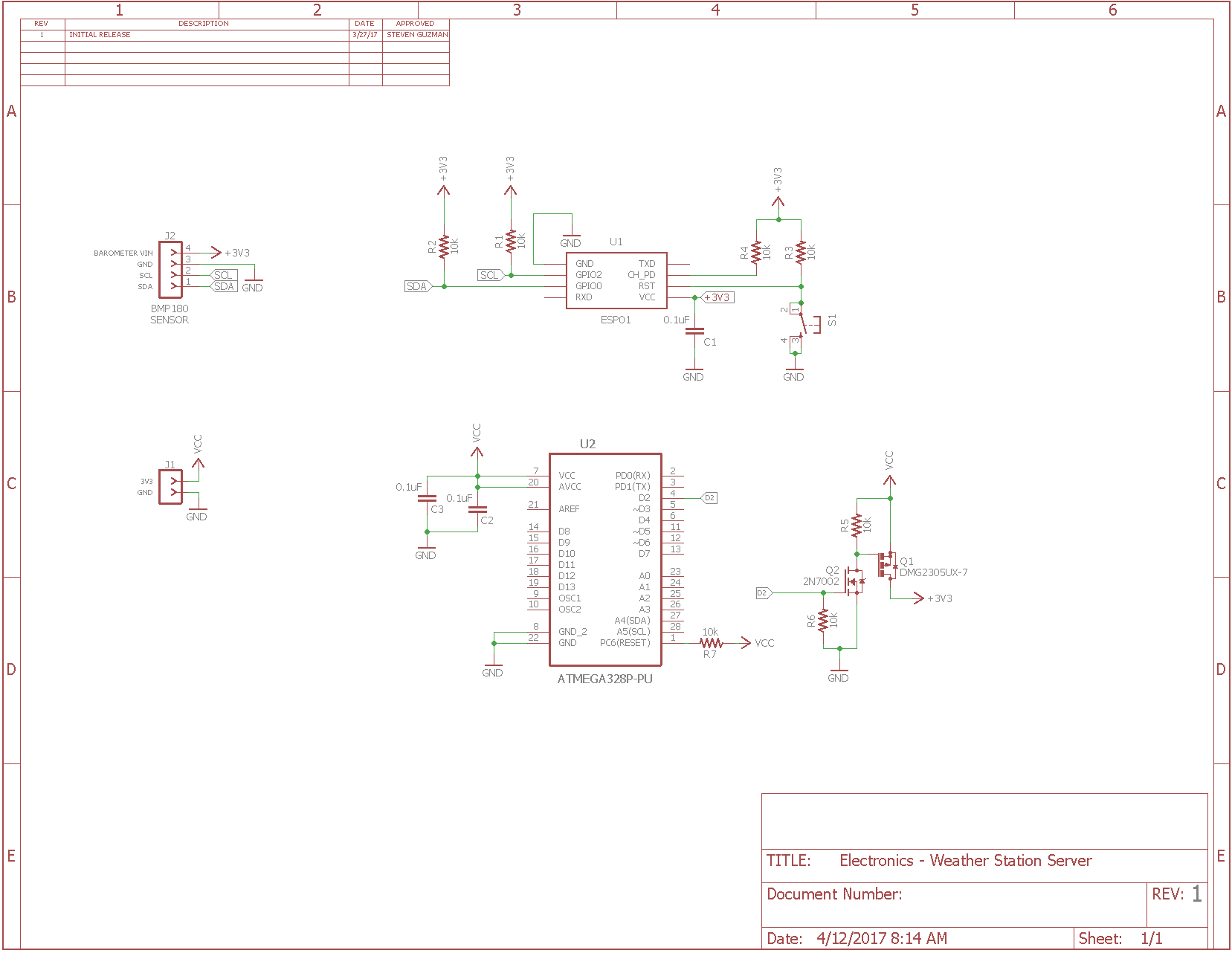
I’ve designed this project to consist of two microcontrollers. Its not the most efficient way of doing it but it is effective. The heart of this project is the ESP8266-ESP01 IC. It will take in the data from the BMP180 sensor over I2C and send the data over to a web hosting site Thingspeak.com
Schematic:
The schematic is not that all complicated but it is very effective at trying to save as much battery as possible and deliver my data for viewing purposes.
In order to have this be powered by 2x AA batteries and last longer then a couple of days or weeks, I needed a couple of things to make this possible which is where the second microcontroller comes into play.
First, we need to make sure we have a stable power supply that can provide up to at least 0.3A and have a minimum quiescent current in the low uA range.
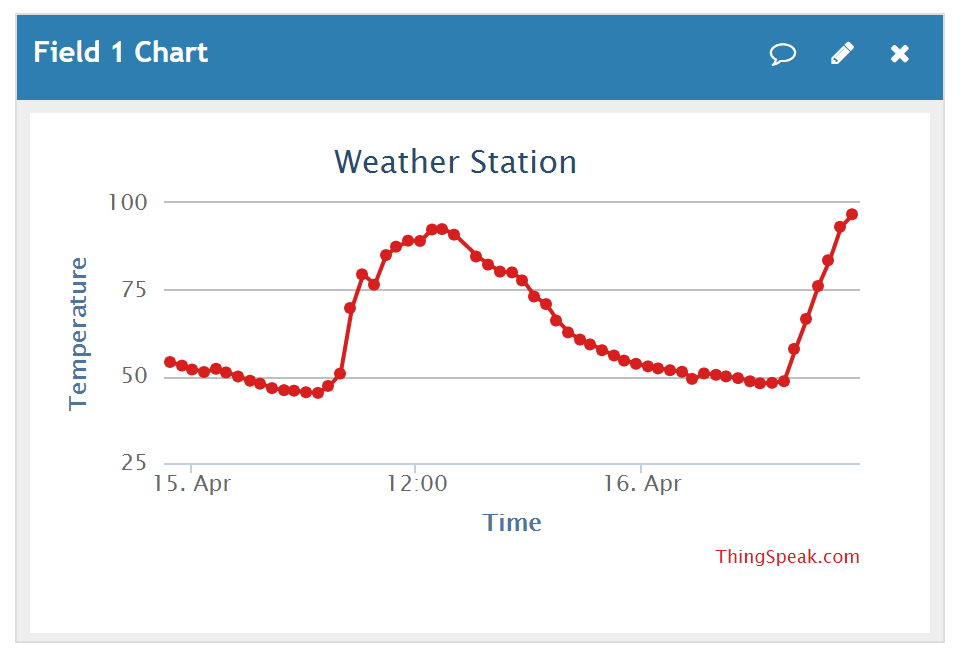
Thingspeak.com
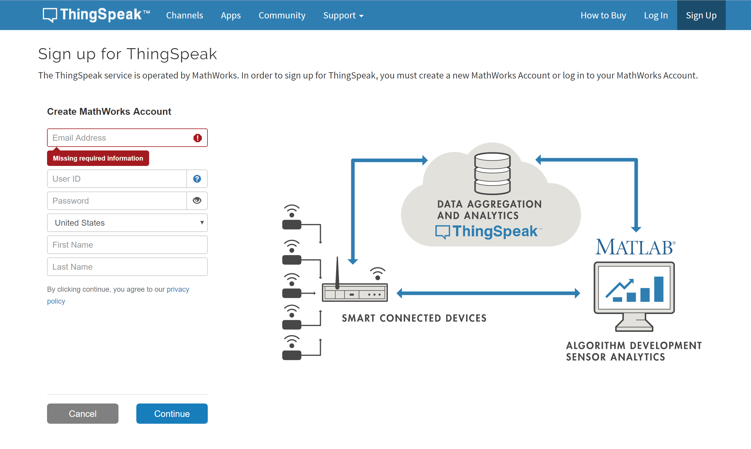
Before we get started into writing the code on the ESP8266 we need to set up an account at thingspeak.
Click on the signup and fill out the information:
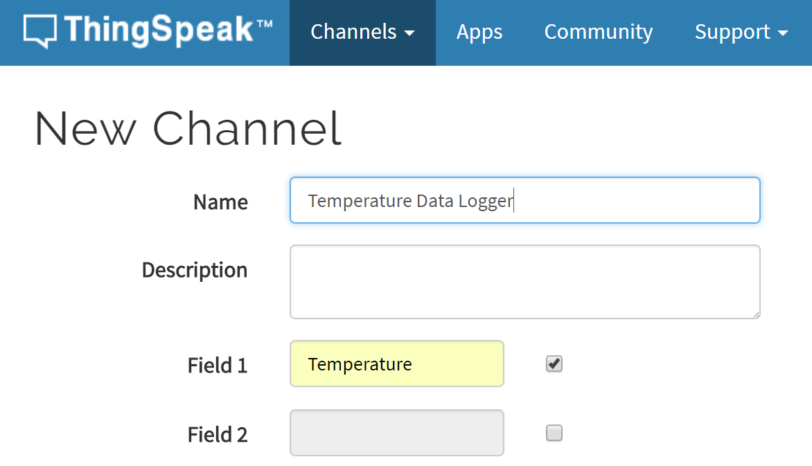
Click on new channel:
The most important information to fill out is the fields, in our case we will fill out field 1 and type in temperature. The name could be any name you want, for this purpose we will write Temperature Data Logger. Once finish, scroll down and click save.
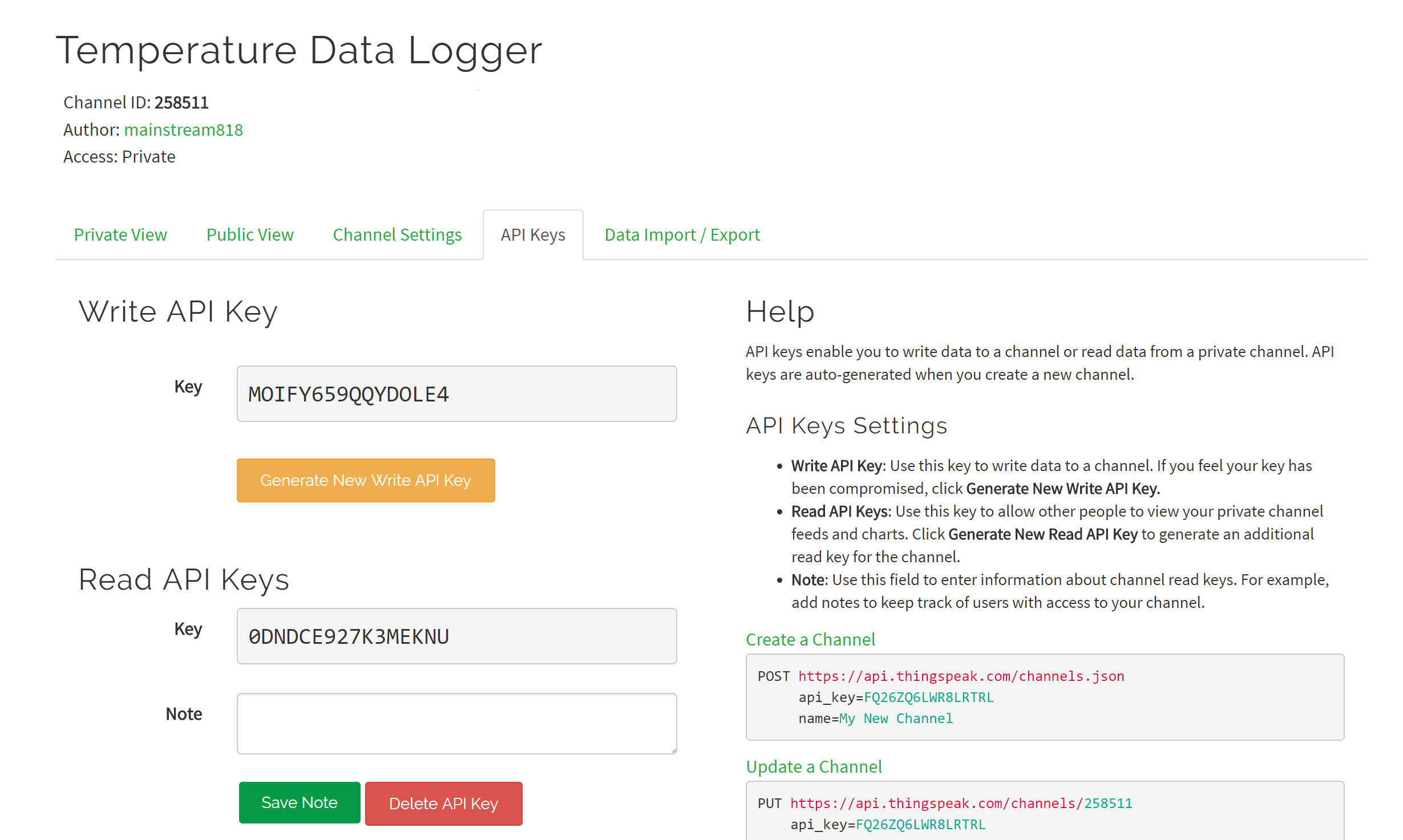
The final piece of information we need is the API key, for this just click on the API Keys button and copy the Write API Key.
Now we can move on to the code.
Click here for step by step on installing the ESP8266 arduino addon.[3]
ESP8266 Code
//////////////////////////////////////////////////////////////////////////////////

// Name: Steven Guzman                                                          //

// Date: 4/4/2017                                                               //

// Description: Temperature webserver that will update every 30 minutes to      //

//              thinkspeak with data that shows the temperature of the inside   //

//              of the enclosure.                                               //

//////////////////////////////////////////////////////////////////////////////////

#include <ESP8266WiFi.h&>

#include <Wire.h>

#include <SFE_BMP180.h>

SFE_BMP180 pressure;

char status;

double t, tf;

// Replace with your channel's thingspeak API key

String apiKey = "";

// Enter your wifi information below

const char* ssid = "";

const char* password  = "";

const char* server = "api.thingspeak.com";

WiFiClient client;

void setup()

{

Serial.begin(115200);

delay(10);

// Pin 0 = SDA

// Pin 2 = SCL

Wire.begin(0,2);

WiFi.begin(ssid,password);

Serial.println();

Serial.println();

Serial.print("Connecting to ");

while (WiFi.status() != WL_CONNECTED)

{

delay(500);

Serial.print(".");

}

Serial.println("");

Serial.println("WiFi Connected");

// Initialize the sensor

if (pressure.begin())

{

Serial.println("BMP180 init success");

}

else

{

Serial.println("BMP180 init fail\n\n");

//while(1);

}

// Print the IP address

Serial.print("Use this URL to connect: ");

Serial.print("http://");

Serial.print(WiFi.localIP());

Serial.println("/");

}

void loop()

{

// This starts the BMP180 sensor and takes a reading

status = pressure.startTemperature();

if (status !=0)

{

delay(status);

status = pressure.getTemperature(t);

}

// Converts Celsius into Farenheid

tf = (9.0/5.0)*t+32.0,2;

if(client.connect(server,80))

{

char t_buffer[10];

// This will convert the double variable into a string

String temp=dtostrf(tf,0,5,t_buffer);

String postStr = apiKey;

postStr +="&field1=";

postStr += String(temp);

postStr +="\r\n\r\n";

client.print("POST /update HTTP/1.1\n");

client.print("Host: api.thingspeak.com\n");

client.print("Connection: close\n");

client.print("X-THINGSPEAKapiKey: "+apiKey+"\n");

client.print("Content-Type: application/x-www-form-urlencoded\n");

client.print("Content-Length: ");

client.print(postStr.length());

client.print("\n\n");

client.print(postStr);

Serial.print("Temperature: ");

Serial.println(t);

Serial.println((9.0/5.0)*t+32.0);

Serial.println(temp);

}

client.stop();

Serial.println("Waiting...");

delay(20000);

}
Arduino Code
///////////////////////////////////////////////////////////////////////////////////////////

/// Title:  Auto Garden Project                                                          //

/// Author: Steven Guzman                                                                //

/// Date:   4/6/17                                                                      //

/// Description: This project will automatically water a plant when the sensor reads low //

///              water levels in the soil.  If sensor reads low water, it will turn on   //

///              boost converter that controls the solenoid valve and then turn on the   //

///              solenoid valve control circuit to allow water to flow into the soil.    //

///////////////////////////////////////////////////////////////////////////////////////////

#include <LowPower.h>

int ESP1 = 2;          // Turns on sensor; set to low for battery consumption purposes (Active High)

void setup()

{

pinMode(ESP1,OUTPUT);     // Configure sensor control as output

digitalWrite(ESP1,LOW);   // Setup as low output

delay(100);

}

void loop()

{

digitalWrite(ESP1,HIGH);  // Turns on the ESP8266

delay(15000);             // 15 second delay

digitalWrite(ESP1,LOW);   // Turns off the ESP8266

// Loops the 8 second internal to extend the sleep state

// 15 = 2 minutes

// 37 = 5 minutes

// 75 = 10 minutes

// 112 = 15 minutes

// 255 = 30 minutes

for(int x = 0; x <= 255; x++)

{

LowPower.powerDown(SLEEP_8S,ADC_OFF,BOD_OFF);

}

}
Programming
ESP8266-ESP01
First things first, we will upload the code to the ESP8266-ESP01. This one is a little bit tricky but after awhile you’ll get the hang of it.
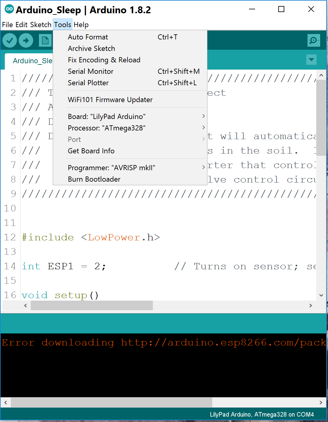
You need to make sure your settings are correct under the Arduino IDE.
See image below:
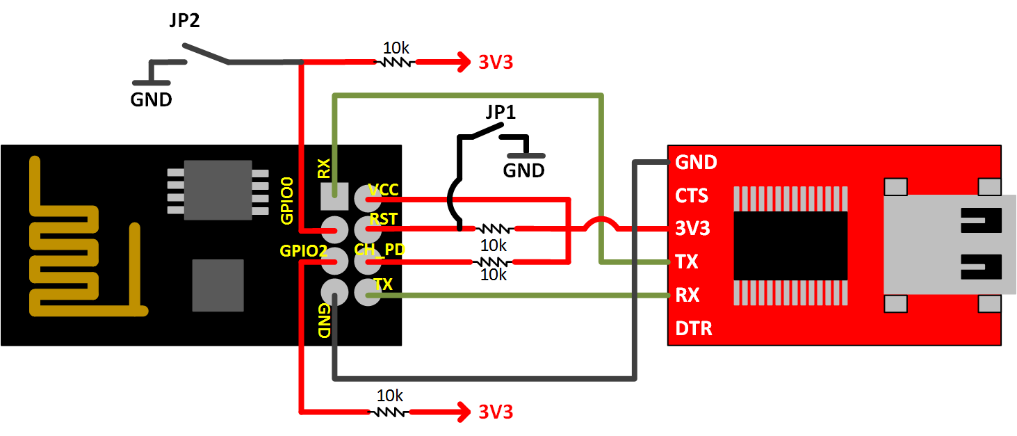
Here’s the wiring diagram for connecting the FTDI programmer to the ESP8266:
Now that your settings are correct, this is were it gets a little tricky to upload the code, you need to follow the steps below in order to upload correctly and successfully
Before hitting upload:
Ground GPIO0 (hold down the push button JP2)
Reset by pulling RST pin to ground (Press and release JP1 button)
Once it restarts, hit the upload sketch icon
When you see compiling sketch switch to uploading, then release the GPIO0 pin
uploading should begin
ATMEGA328P-PU (ARDUINO LILYPAD)
Next, we will upload the second code into the ATmega328 which has the lilypad bootloader installed ( Click HERE[2] for tutorial on flashing ATMEGA328P-PU with bootloader).
See image below for settings:
Final Thoughts and Future updates
And now the final product:
Its not the most elegant but I actually used my CNC machine to make these boards, in the future I might get them professionally made but for now its perfect for me.
Future Updates:
Replace the ATMEGA328P-PU IC with a smaller ATTINY85 which can also be flashed with the Arduino bootloader
Connect the Arduino to the I2C communication lines to expand its data logging capability
Since this is running on 2x AA NiMH batteries, it would be great to monitor battery capacity. We can use one of the analog pins on the arduino to read the data and send it over I2C to the ESP8266