Here is a new project I’m working on and hoping to get to a point where I can share the files and source code.
This is a replacement for a passive DC fuse box that you typically buy for low power solar projects.
This will allow you to remotely control 6 independent circuits each with a dedicated 25A max blade fuse. It uses an esp32 pico and each circuit has a 31A max current sensor. With the esp32, data logging can be incorporated and sent to influxDB server.
I’m very excited and hopefully I can get this project done so you can enjoy it as well
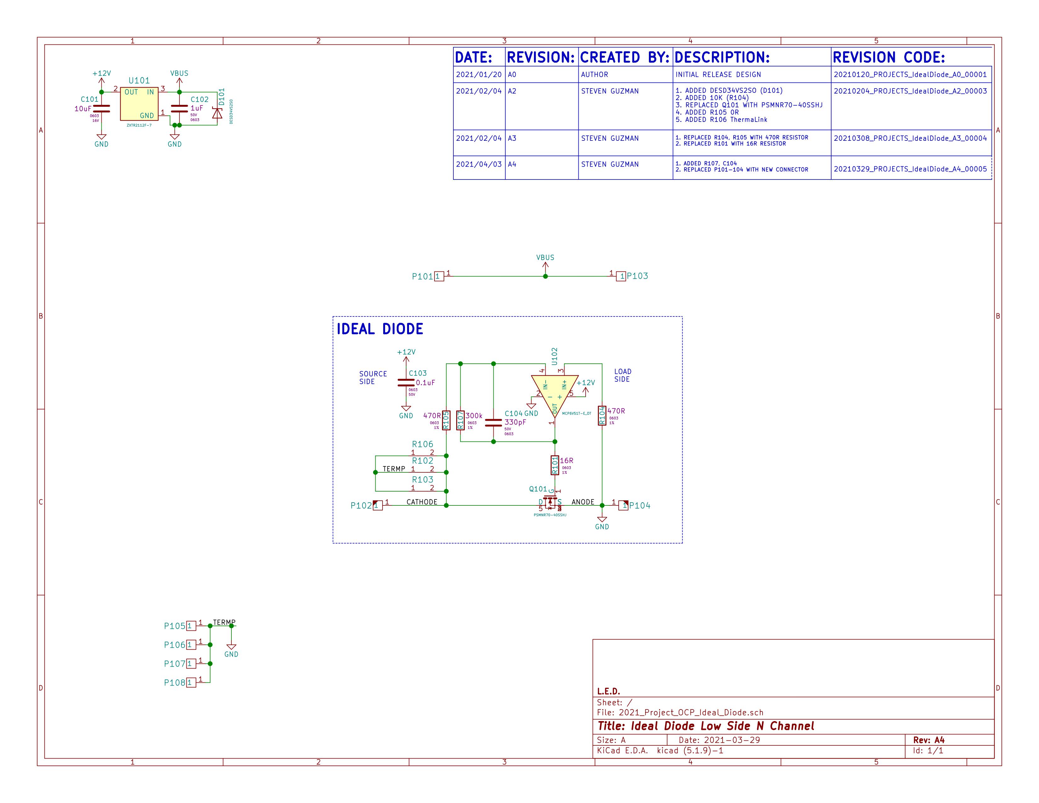
Replaced P102,P104 pads with high current part# 7460305
Added R107 (300k) and C104 (330pF) for better stability by lowering the gain
Update (All updates are already included in the github files, link at the end):
Updated R104, R105 to resistor value 470ohms for better reverse current protection threshold
Updated R101 to resistor value 16ohms for better stability
WHAT IS THIS?
What is an ideal diode? An ideal diode operates exactly as a traditional blocking diode that’s used to reverse current protection for a power path to protect the source from become the load and absorb power.
The only downside to using a diode is the power loss since most Shottky diodes, which is the a type of diode used primarily in power circuits, have a minimum voltage drop of 0.4V to allow current flow. This is an issue if you are trying to pass 50A through the diode which is a power loss of 10W which is a significant on design to eliminate that much heat from the diode.
The solution is to use is to use the ideal diode as a replacement for the Shottky diode. The ideal diode in summary is a linear op amp driving a mosfet with a low RDson internal resistance to turn on when current is flowing to the load and turn off when current tries to flow back to the source.
WHY DO WE NEED THIS?
Why is this circuit used and why is it needed?
The primary reason why I looked into this and designed this circuit was to have the ability to parallel multiple battery banks without having to worry if one of the banks ended up shorting out or having some fault that triggered the BMS system to turn off that particular bank.
This circuit is also known as an OR-ing diode because it allows the use of multiple parallel sources to help drive the load and the load alone. If one source has an issue then it can be removed without having to turn off the system to do so and in the case of a battery bank, it keeps it from either being charged from the other batteries in parallel in case of an over voltage condition and it keeps it from discharging to other banks in case of an under voltage condition.
HOW DO WE CREATE THIS?
How is this circuit made? Below I’ve created a discrete ideal diode using an op amp for driving and a Mosfet as the diode switch.
SPECIFICATION
Vinmin: 14V
Vinmax: 36V (This is limited by the mosfet and tvs diode, change those parts to increase input voltage range)
Imax: 30A ( This is dependent on the mosfet that is chosen, this rating is without a heatsink. I will perform test when I receive the actual boards as I used 2oz copper and should be able to handle more current without an issue. In theory this mosfet should be able to handle 400A with a proper heatsink)
SCHEMATIC
RENDERING
FRONT SIDE PCB
BACK SIDE PCB
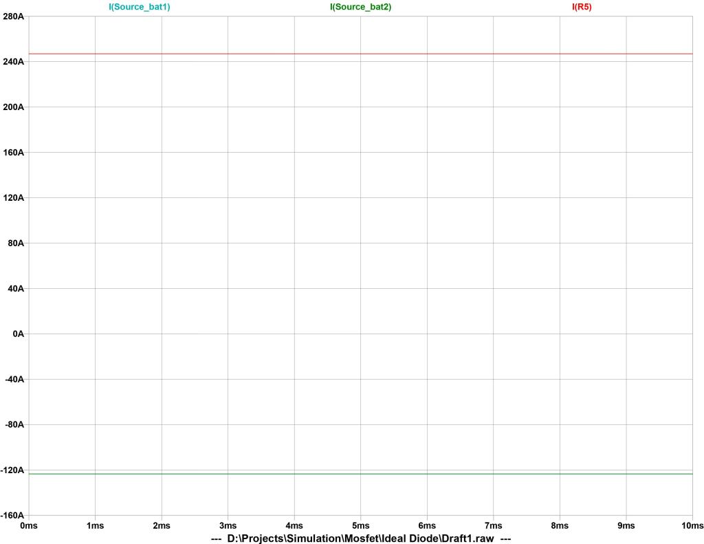
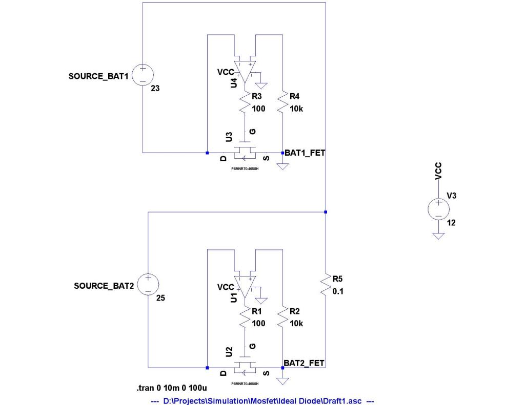
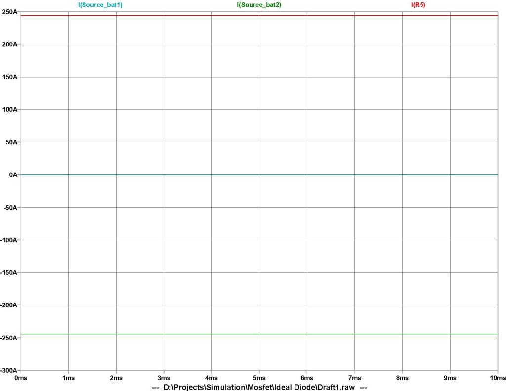
SIMULATION
Below I also simulated the circuit and you can see what both the sources share the current when they are equal in voltage. But when source “BAT01” drops in voltage, which simulates either a faster discharge on that parallel cell or the bms turned off the battery pack due to a fault event, source “BAT02” is now providing all the current to the load. You can see that BAT01 ideal diode is blocking the current from charging the battery which is known as reverse current.
WHERECAN I DOWNLOAD THIS?
I’ve uploaded all the files, which included sources files and gerber, on my github below: