

Transistors, specifically MOSFETs, I would say are the second most important component to an EE designer next to the passive compoents (resistors, inductors, capacitors).
I will show you a few useful applications that can be applied using MOSFETs that anyone working in electronics should have in there arsenal.
First lets briefly look at the two variations of MOSFETs.
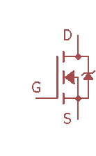
You have the N-Channel MOSFET below:
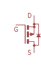
Then, you have the P-Channel MOSFET below:
They have some minor differences in the way they are made and how they are used but in essences they have the same function and operate the same.
Every MOSFET has a Gate-source threshold voltage 
Now, onto the main event:
1. Using them as digitally controlled switches.
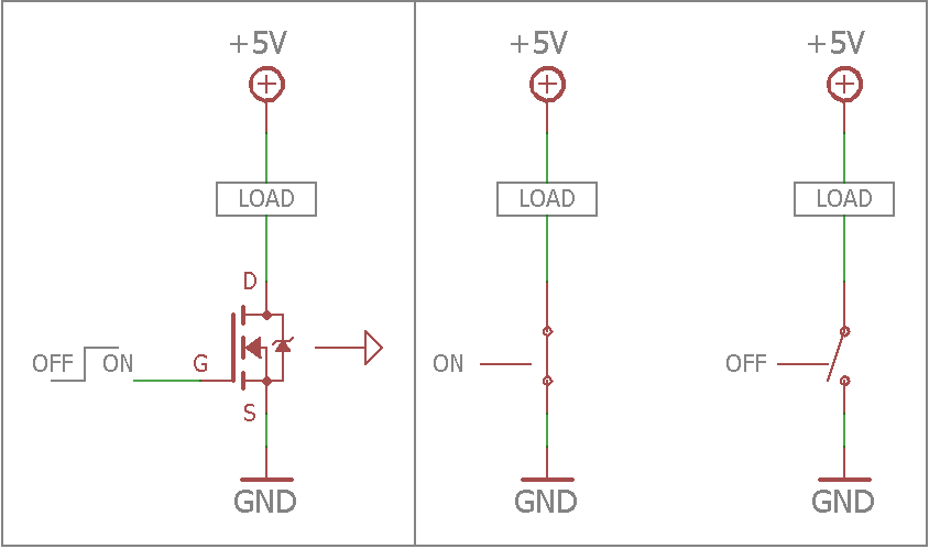
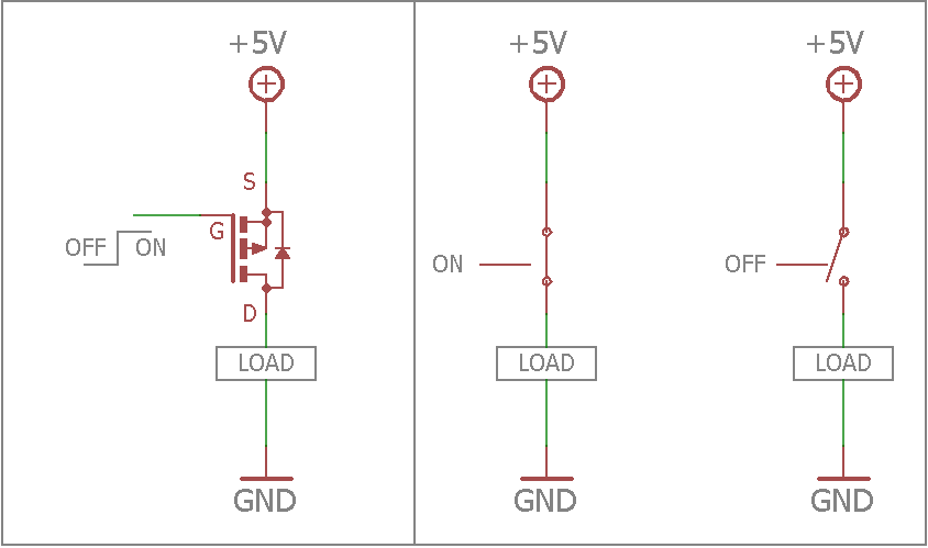
One of the most common uses for these FETs is to use them as switches. When working with electronics, especially with battery operated electronics, you sometimes need to control when certain sensors are turned on or control when certain components get powered on in order to conserve battery power.
Here comes the FETs to the rescue.
You have two ways of accomplishing this task, using either the NMOS or the PMOS.
Note: When using MOSFETs with digital electronics, make sure you get a logic level mosfet. Meaning that the on voltage for Vgs is between 2V-5V.
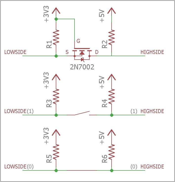
Using the NMOS, this is considered LOW SIDE switching because the source pin is connected to ground.
Using the PMOS, this is considered HIGH SIDE switching because the source pin is connected to the device/component instead of ground.
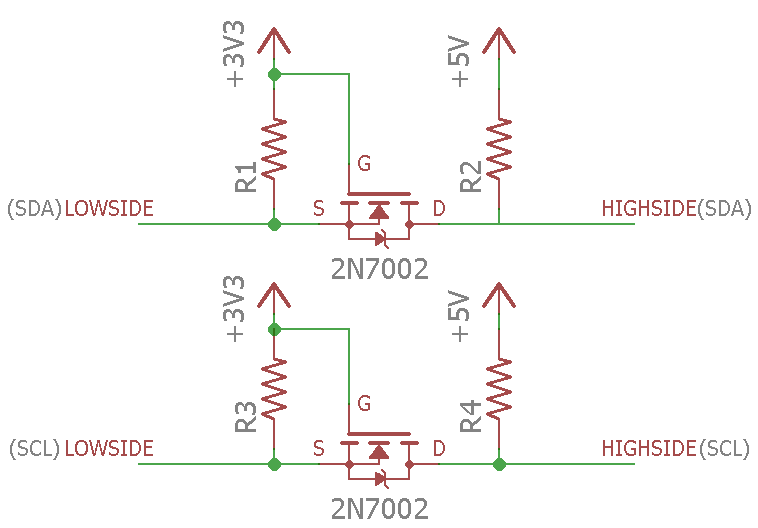
2. Using them as logic level converters[1]
This one mostly applies to the NMOS MOSFET, I haven’t seen a configuration out there with PMOS.
Nowadays with DIY electronics being more and more popular and with a larger community of makers, you have a huge variety of microcontrollers and sensors to make the next big product. With this variant comes a variety of components with different supply voltages, ranging down from 1.8V up to 5V. The issue with this is trying to match sensor supply voltages with your microcontroller when it comes to communicatong via I2C or SPI or even a single 1 or 0 signal. If you supply a sensor or IC with a higher signal voltage than it can handle you risk damaging the component and rendering it useless.
Here comes the NMOS to the rescue. With an NMOS you can fix this issue by making a 5V to 3.3V logic level shifter to communicate with each other while avoiding any damage.
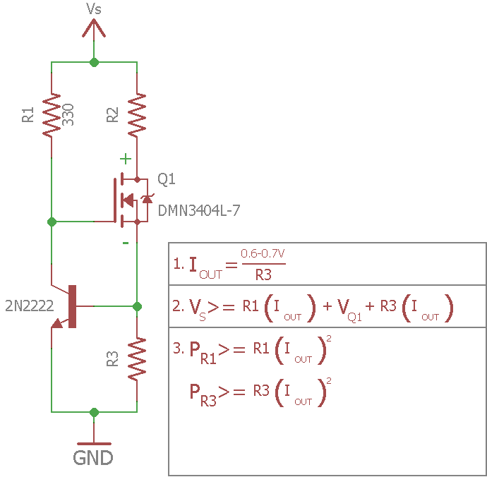
3. Making a constant current source.
This is one is my favorite application using MOSFETs. For me I do a lot of testing of DC DC Converters to make sure it meets my design specifications and one test requires I have a constant current that will not fluctuate. Using this design I am able to set the desired current for my test.
Another application is used for LEDs. LEDs are a lot different that traditional light bulbs in that instead of operating off a voltage rating, they operate at a current rating. Essentially you need to maintain a constant current applied to the LED to achieve your desired brightness.
These are some of the three uses for MOSFETs that I normally deal with for my projects. There’s plenty more but these were my top 3.
If you have any questions, input, corrections, please let me know in the comments below.
Enjoy building :)!
References:


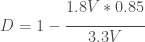 = 0.52
 = 0.36
 = 0.22A
 = 0.165A
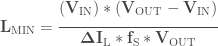
 – This is the switching frequency that the converter will operate at.
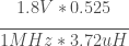
 = 3.72uH
 = 3.97uH
 = 0.19A
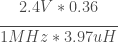 = 0.18A
 =
= 
 – This is the current switch limit of the boost converter.
 =
=  = 0.33A
 = 0.45A
 the Inductor will see. This value cannot exceed the ILIM value of the boost converter:
 = 0.94A
 = 0.72A
 value cannot exceed
  which can be found in the datasheet. In this example we see that with a low input voltage, the switching current exceeds the limit in the datasheet. The boost converter might still be able to output the desired current at that low input voltage because
 – This is the current that the feedback resistor draws.
 – This is the feedback reference voltage
 = 35mA
 = 35.4kΩ
 = 58.74kΩ
 : Typically this value is 4.7uF to 10uF
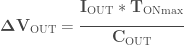
 – This is the maximum on time of the boost converter. It is also written as


 = 50uF
 = 50mV
 = 37mV
 = 87mV